


お知らせ
「H2& FC EXPO【春】第25回 [国際] 水素・燃料電池展」に出展いたします

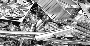
Precious metals
give possibilities for the future.
Again and again.
「H2& FC EXPO【春】第25回 [国際] 水素・燃料電池展」に出展いたします
田中貴金属工業、100℃前後で高い水素透過性能を示す高性能パラジウム水素透過膜の開発に世界で初めて成功
Metalor Technologies SA Completes Acquisition of Gannon & Scott
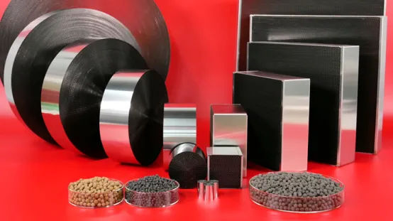
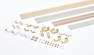
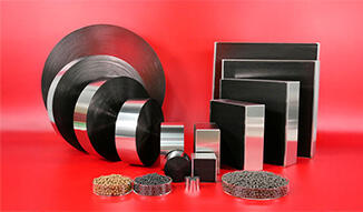
TANAKA PRECIOUS METAL TECHNOLOGIES Establishes Transfer Technology for Sintered Gold (Au) Bonding Technology AuRoFUSE™ Preforms
TANAKA PRECIOUS METAL TECHNOLOGIES Establishes Total Solutions System for Contract Manufacturing of Various Test Kits, including In-Vitro Diagnostic Reagents
TANAKA to Exhibit at "H2 & FC EXPO [March] - 25th International Hydrogen & Fuel Cell Expo"
TANAKA Develops World's First High-Performance Palladium Hydrogen Permeable Membrane Exhibiting High Hydrogen Purification Performance at Temperatures around 100℃
Metalor Technologies announced today that, following approval by the relevant regulatory authorities, it has completed the previously announced acquisition of Gannon & Scott.
TANAKA Establishes Transfer Technology for its Sintered Gold (Au) Bonding Technology "AuRoFUSE™ Preforms"
TANAKA PRECIOUS METAL TECHNOLOGIES establishes total solutions system for contract manufacturing of various test kits including in vitro diagnostics
TANAKA entwickelt weltweit erste wasserstoffdurchlässige Hochleistungs-Palladium- Membran mit hoher Reinigungsleistung bei Temperaturen um 100 °C
TANAKA präsentiert Transfertechnologie für AuRoFUSE™ Preforms
Metalor Technologies announced today that, following approval by the relevant regulatory authorities, it has completed the previously announced acquisition of Gannon & Scott.
TANAKA PRECIOUS METAL TECHNOLOGIES Establishes Comprehensive Total Solution System for Contract Manufacturing of Test Kits, including In Vitro Diagnostics
TANAKA's Group Company EEJA to Exhibit at the 40th NEPCON JAPAN
TANAKA PRECIOUS METAL TECHNOLOGIES, 100℃ 전후에서 높은 수소 투과 성능을 보이는 고성능 팔라듐 수소 투과막 개발에 세계 최초로 성공
Metalor Technologies announced today that, following approval by the relevant regulatory authorities, it has completed the previously announced acquisition of Gannon & Scott.
TANAKA PRECIOUS METAL TECHNOLOGIES, 'AuRoFUSE™ Preforms'
TANAKA PRECIOUS METAL TECHNOLOGIES Establishes Total Solution System for Consigned Manufacturing of In Vitro Diagnostic Drugs and Various Test Kits
TANAKA's Group Company EEJA to Exhibit at the 40th NEPCON JAPAN
Metalor Technologies announced today that, following approval by the relevant regulatory authorities, it has completed the previously announced acquisition of Gannon & Scott.
TANAKA PRECIOUS METAL TECHNOLOGIES Established thermal metal (Au) bonding technology "AuRoFUSE™ Preforms" branding technology
TANAKA PRECIOUS METAL TECHNOLOGIES establishes a comprehensive solution system for contract manufacturing of various test kits, including in vitro diagnostic reagents
TANAKA's Group Company EEJA to Exhibit at the 40th NEPCON JAPAN
TANAKA will Exhibit at MD&M West 2026 in Anaheim, CA from February 3rd to 5th, 2026
TANAKA PRECIOUS METAL TECHNOLOGIES 成功開發出世界首創在100℃左右具有較高的氫氣過濾性能之高性能濾氫鈀膜
Metalor Technologies announced today that, following approval by the relevant regulatory authorities, it has completed the previously announced acquisition of Gannon & Scott.
TANAKA PRECIOUS METAL TECHNOLOGIES Establishes Transfer Technology for Au Sintered Bonding Technology
TANAKA PRECIOUS METAL TECHNOLOGIES has established a comprehensive solution system for various testing kits, including those for in vitro diagnostic reagents, upon request.
TANAKA's Group Company EEJA to Exhibit at the 40th NEPCON JAPAN