
TANAKA Insights

TANAKA has been widely developing its business centered on precious metals since its founding in 1885. Currently, about 70% of its business is related to precious metal materials for industrial use...
New Articles
Latest articles from TANAKA.
- Consumer Electronics
- Semiconductor
- Thin Films/Deposition
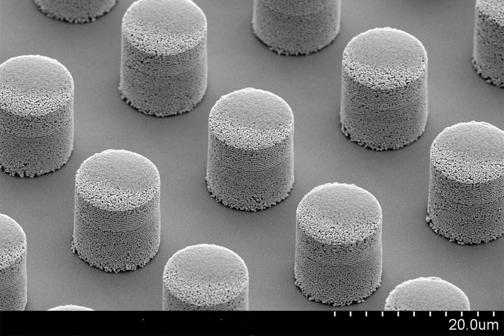
EDITOR`S PICKS: TANAKA Establishes Transfer Technology for its Sintered Gold Bonding Technology
Source: Semiconductor Digest Date: February 3, 2026 Written by: Semi...

- Medical
- Medical Device Materials
MD&M West 2026 Booth Briefing—Silver-Based Materials for High-Precision, Minimally Invasive MedTech
This image is for illustrative purposes. Source: Machine Design Date: February 2, 2026 ...
- Consumer Electronics
- Semiconductor
- Joining and Sealing (Packaging)
- Relays and Electrical Contacts
Material innovation: The new frontier of industrial automation
This image is for illustrative purposes. Source: Asia Pacific Metalworking Equ...

- Consumer Electronics
- Semiconductor
- Joining and Sealing (Packaging)
- Relays and Electrical Contacts
Source: Electronics For You BUSINESS – News
- Consumer Electronics
- Semiconductor
- Joining and Sealing (Packaging)
- Relays and Electrical Contacts
Source: Semiconductor Digest Date: December 12, 2025 Link:...
- Consumer Electronics
- Semiconductor
- Joining and Sealing (Packaging)
- Relays and Electrical Contacts
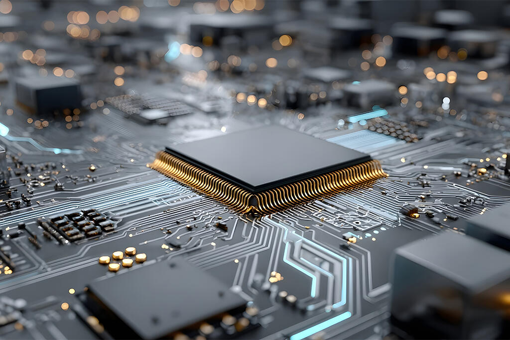
TANAKA PRECIOUS METAL TECHNOLOGIES Kogyo, the "mediator" between heterogeneous chips and substrates, is a member of the semiconductor post-processing...
- Consumer Electronics
- Semiconductor
- Joining and Sealing (Packaging)
- Relays and Electrical Contacts
Currently, in semiconductor back-end processes, the introduction of new technologies that are expected to be epoch-making, mainly in packaging technology, is being...
- Consumer Electronics
- Semiconductor
- Joining and Sealing (Packaging)
- Relays and Electrical Contacts
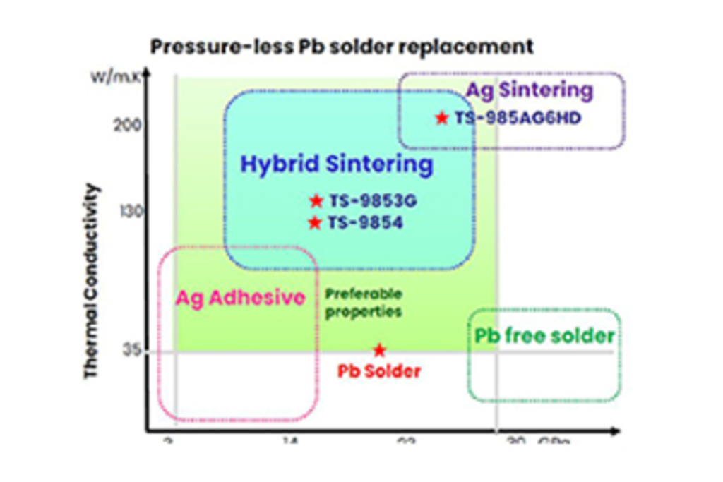
TANAKA is strengthening its semiconductor-related business. Drawing on its expertise in precious metals developed through many years of experience, the Group is...
- Consumer Electronics
- Semiconductor
- Joining and Sealing (Packaging)
- Relays and Electrical Contacts
December 10, 2025 Nikkei MOOK Since its founding in 1885, TANAKA has been involved in a wide range of...
- Consumer Electronics
- Semiconductor
- Joining and Sealing (Packaging)
- Relays and Electrical Contacts
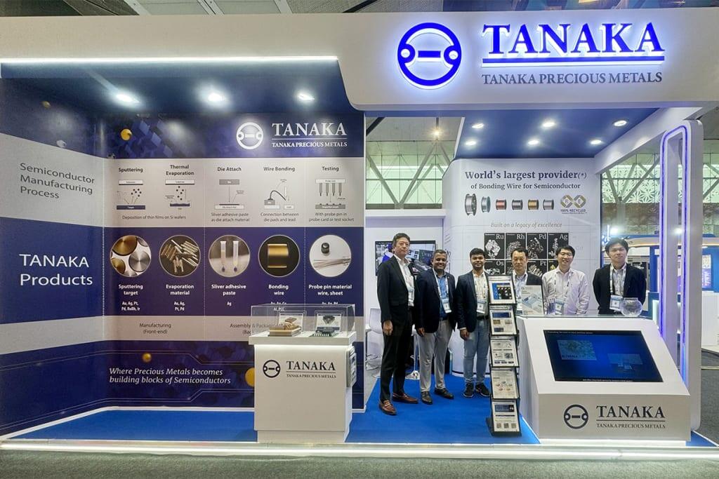
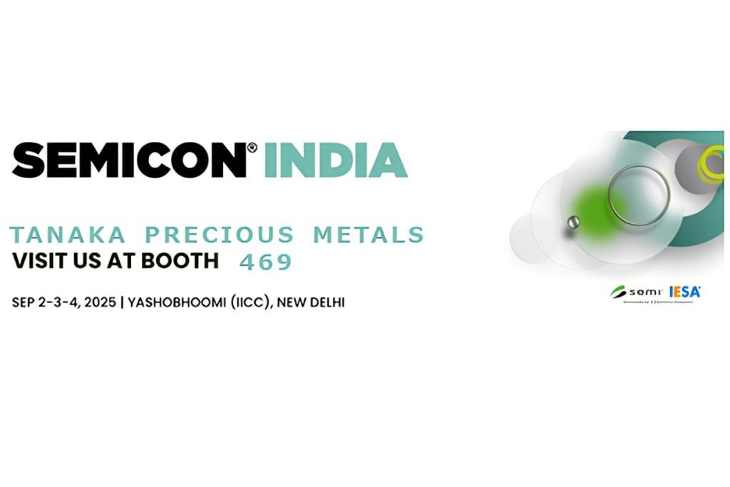
Supporting India's Semiconductor Growth with High-Performance Precious Metal Materials - TANAKA
Source: DataQuest India Date: September 9, 2025 Link: Support...
Search Articles
- Search by keyword
-
- Frequently searched keywords
- Find by Industry
- Search by Product Use and Function