
The Future Enabled by Bonding Technology Using AuRoFUSE™

Semiconductor Packaging Technology Using Gold Nano Paste
~Stable LED Lighting, Power Devices, and MEMS through Low-Temperature Bonding and High Reliability
Researchers and Developers

TANAKA PRECIOUS METAL TECHNOLOGIES
Metal Materials Development Department
Unlike conventional silver paste, materials made from gold nanoparticles in paste form have overwhelmingly higher reliability and can be used as lead-free materials since they can be processed at 200°C without pressure, resulting in lower processing costs. Ultimately, since gold nanoparticles are directly bonded to each other, the thermal conductivity is also higher than that of silver fusion using silver paste, making it easier for heat to escape. Although gold is generally associated with high cost, when the overall advantages in terms of processing efficiency, manufacturing equipment costs, high reliability (long lifespan), replacement costs, and performance (high output of power devices) are converted into costs, the system cost may actually be lower.
TANAKA PRECIOUS METAL TECHNOLOGIES has developed a new gold nanoparticle paste material, "AuRoFUSE," and is proposing its application in semiconductor packaging technology. Due to its high adhesion and work efficiency, it is expected to be used in power device die bonding and wafer bonding in wafer-level packaging (WLP).
Gold is extremely stable in nature and has been used in shrines, temples, and cultural properties from as far back as 1,000 years ago. The same is true in the world of semiconductors and electronics, where, for example, printed circuit boards for smartphones and mobile phones are used in large quantities to the extent that they are jokingly referred to as "urban mines." This is because gold has unique properties that prevent rust and deterioration. In electronic circuits, rust increases resistance, and unintended metal growth can lead to short circuits. Repeatedly subjecting them to high and low temperatures in actual use can cause cracking and peeling. However, gold does not undergo the same changes over time as other metals. It remains stable for many years.
On the other hand, in the world of electronic circuits, lead-free solders have been developed for joining metals without using the harmful lead solder. However, there has been a restriction that processing must be done at temperatures 30 to 40°C higher than those of conventional lead solders. As a result, manufacturing equipment became expensive, and the manufacturing process was also complicated. Achieving lead-free bonding at temperatures close to those of lead solder has been one of the major goals in metal bonding.
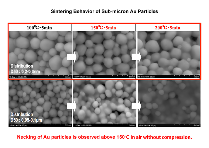
Gold paste that can be used for bonding at 200℃
TANAKA's AuRoFUSE is a gold paste that can be used for bonding at 200℃, which is lower than the bonding temperature of lead solder (Figure 1). This gold paste uses nanoparticles with a particle size of 200 to 400 nm, as this size is considered optimal for mounting semiconductor chips. If the particle size is smaller than this size, necking, a phenomenon in which nanoparticles tend to stick together, occurs at around 150℃, making it difficult to handle. If the particle size is larger and 1 µm or more, the melting temperature will reach 400℃, making it difficult to use.
In conventional gold pastes, gold particles are dissolved in organic solvents, and dispersants are added to adjust the viscosity of the paste. High viscosity makes the paste difficult to use, and viscosity that is moderate and not as liquid is the easiest to process.
In this case, the particle size is controlled between 200 and 400 nm, and only surfactants are used as solvents. This means that there is no need to adjust viscosity, and it can be set to an easy-to-use viscosity. The basic idea is that the surfactant moderately covers the surface of the gold particles and peels off easily at temperatures above 100°C. The gold particles and surfactants are physically attached, but not chemically bonded. Therefore, when heat is applied, the surfactant peels off easily.
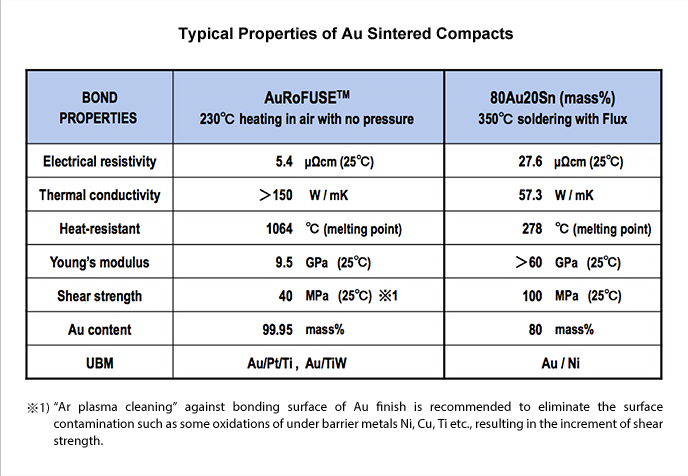
Compared to AuSn eutectic solder, which is one of the lead-free solders, AuRoFUSE has a lower electrical resistivity of 5.4 µΩcm (25°C), which is 1/5 of that of AuSn eutectic solder, and a higher thermal conductivity of over 150 W/mK, which is three times that of AuSn eutectic solder (Table 1). This means that both heat and electricity can flow easily. In addition, it has a low Young's modulus of 9.5 GPa, which is less than 1/6, indicating that it is a soft material. Soft materials also have the advantage of absorbing stress. When compared to AuSn eutectic solder, it can be used as a contact material with silicon as before, with Ti as the barrier metal, and Pt or TiW as the barrier metal.
When using this gold nano paste for die bonding chips, Au/Pd/Ni metal should be formed on semiconductor chips and substrates, including adhesion to substrates and compatibility of thermal expansion coefficients. Then, at the position where AuRoFUSE is to be mounted, Au is dispensed from a dispenser and attached to the Au/Pd/Ni metal layer (Figure 2). After that, pressure is applied and heat treatment is performed to bond them. The bonding time is about 20 minutes at 200 to 230°C. Post-sintering is performed for 1 to 3 hours after bonding to stabilize the bonding part.

Expected applications of this gold nano paste include LED headlight lighting, laser headlights (Reference 1), laser projectors, and GaN power devices used in front lights of vehicles.
Be careful of heat dissipation
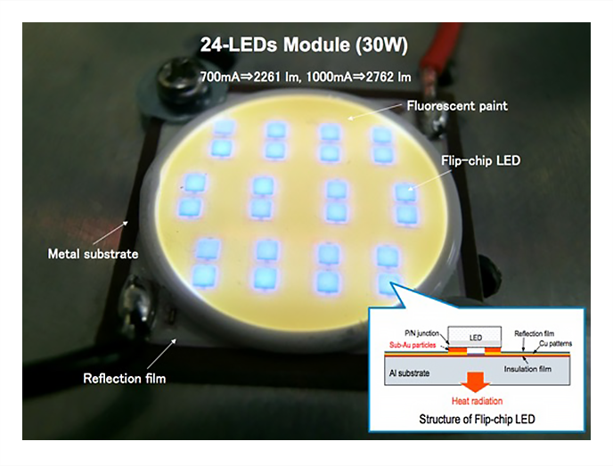
LED lighting uses a method of arranging multiple LEDs in a row to emit light. In LED lighting, blue LEDs are coated with yellow phosphor, and blue + yellow are used to create white. Figure 3 shows an LED lamp equipped with a total of 24 LED chips, with 12 pairs connected in series and connected in parallel. Here, the chips are mounted face down on an aluminum substrate. The aluminum substrate under the bonding pad of the face-down chip is electrically insulated from the bonding pad using an insulating sheet, but since only heat needs to be released, materials with good thermal conductivity must be used between the aluminum substrate and the bonding pad. The heat from the LED is released through the aluminum substrate, and the n and p electrodes of the LED are designed to release heat to the outside.
An on/off test (24V, 350mA, 15-minute rest period) was conducted on eight LED modules with this structure. Three prototypes were made for the bonding pads: Au paste, AuSn solder, and SnAgCu solder, and eight of each were tested. All AuSn solder modules failed after 500 cycles, and only three SnAgCu solder modules survived after 1000 cycles. They were able to survive 3000 cycles, but only two survived after 4000 cycles, and all failed after 5000 cycles. However, none of the Au paste electrodes failed even after 15,000 cycles.
For laser diodes, an AuZn layer, a Ti layer, and an Au layer are provided from the chip side as electrode layers on the substrate side of the laser chip, and an Au film is formed on the copper substrate, and the Au layers are bonded together using the AuRoFUSE Au paste. Because the bonded parts are Au-to-Au, no potential difference occurs, so there is no need to worry about reliability issues. By bonding at 200°C or higher and then sintering, the solvent contained in the gold paste evaporates, leaving only pure gold to bond, resulting in a very stable gold-to-gold bond.
The reason why GaN devices are considered promising as heat-generating power devices is that they are devices that pass current horizontally. If Ag (silver) is used for die bonding, the potential difference with the Au bonding wire can cause Ag migration, which can lead to the growth of dendrites and short circuits between terminals. For this reason, Au-Au bonding is preferable. However, because SiC transistors are types that pass current vertically, there is little risk of short circuits even if migration occurs when Ag is used as the die bonding material. For this reason, there is little motivation to use Au for SiC devices.
Applications for WLP Packages
Another application of AuRoFUSE is as a vacuum sealing material for WLP packages. When mass-producing sensors that form thin membrane films to measure their capacitance and piezo-resistance, such as MEMS devices, MEMS chips are encapsulated in molding resin using hermetic sealing.
In the future, if WLP can be used to create smaller and more corrosion-resistant packages, it may be possible to use them for bio-implantable sensors. A cap wafer is placed over a device wafer for sealing, and if gold is used to seal between the wafers, it will not corrode even in the body.
TANAKA has developed a technology that forms patterns on transfer wafers using lithography and then transfers those patterns onto the gold patterns of device wafers. Transfer wafers can be reused multiple times, so there is no waste.

When using a gold pattern as a frame for sealing, it has the advantage that a slightly rough surface of the substrate can still be followed without creating gaps. Gold undergoes sintering and deforms according to the substrate. Figure 4 shows a pattern (right in Figure 4) and a cross-sectional view (left in Figure 4) after hermetic sealing by thermocompression bonding gold at 200°C and 100 MPa. This method also has the advantage that a gold frame for hermetic sealing and gold connections for electrodes can be formed simultaneously, which may facilitate the integration of 3D ICs with MEMS through TSV (Through Silicon Via) in the future.
Reference Material
1. The Laserlight, the latest headlight installed in the BMW i8 and the new 7 Series, is amazing
Press Release
We introduce the potential of precious metals in various fields.

TANAKA handles everything from procurement of bullion to supply of materials, research and development, manufacturing, sales, and recycling.
We offer a full range of services related to precious metals, and by combining them optimally, we provide total solutions tailored to our customers' needs.
How was this article?
If you found this helpful, please share it.