CLOSE
About Elements
TANAKA is a leading company in the field of precious metals.
Advanced materials and solutions that support societal progress, the development stories behind them, the voices of engineers, and our management philosophy and vision—
Elements is an online media platform that shares insights that lead to a better society and a more prosperous future for the planet under the slogan “Mastering Precious Metals.”

Researchers create breakthrough spintronics manufacturing process that could revolutionize the electronics industry

University of Minnesota Twin Cities researchers, along with a team at the National Institute of Standards and Technology (NIST), have developed a breakthrough process for making spintronic devices that has the potential to become the new industry standard for semiconductors chips that make up computers, smartphones, and many other electronics. The new process will allow for faster, more efficient spintronics devices that can be scaled down smaller than ever before.
The researchers’ paper is published in Advanced Functional Materials, a peer-reviewed, top-tier materials science journal.
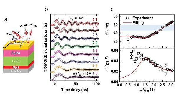
Schematic illustration of the TR-MOKE measurements
“We believe we’ve found a material and a device that will allow the semiconducting industry to move forward with more opportunities in spintronics that weren’t there before for memory and computing applications,” said Jian-Ping Wang, senior author of the paper and professor and Robert F. Hartmann Chair in the University of Minnesota Department of Electrical and Computer Engineering. “Spintronics is incredibly important for building microelectronics with new functionalities.”
Wang said Minnesota has been leading this effort in a big way for more than 10 years with strong support by the Semiconductor Research Corporation (SRC), Defense Advanced Research Projects Agency (DARPA), and the National Science Foundation (NSF).
Wang’s team has also worked with University of Minnesota Technology Commercialization and NIST to patent this technology, along with several other patents related to this research. This discovery also opens up a new vein of research for designing and manufacturing spintronic devices for the next decade.
“This means Honeywell, Skywater, Globalfoundries, Intel, and companies like them can integrate this material into their semiconductor manufacturing processes and products,” Wang said. “That’s very exciting because engineers in the industry will be able to design even more powerful systems.”
The semiconductor industry is constantly trying to develop smaller and smaller chips that can maximize energy efficiency, computing speed, and data storage capacity in electronic devices. Spintronic devices, which leverage the spin of electrons rather than the electrical charge to store data, provide a promising and more efficient alternative to traditional transistor-based chips. These materials also have the potential to be non-volatile, meaning they require less power and can store memory and perform computing even after you remove their power source.
Spintronic materials have been successfully integrated into semiconductor chips for more than a decade now, but the industry standard spintronic material, cobalt iron boron, has reached a limit in its scalability. Currently, engineers are unable to make devices smaller than 20 nanometers without losing their ability to store data.
The University of Minnesota researchers have circumvented this problem by showing that iron palladium, an alternative material to cobalt iron boron that requires less energy and has the potential for more data storage, can be scaled down to sizes as small as five nanometers.
And, for the first time, the researchers were able to grow iron palladium on a silicon wafer using an 8-inch wafer-capable multi-chamber ultrahigh vacuum sputtering system, a one-of-a-kind piece of equipment among academic institutions across the country and only available at the University of Minnesota.
“This work is showing for the first time in the world that you can grow this material, which can be scaled down to smaller than five nanometers, on top of a semiconductor industry-compatible substrate, so-called CMOS+X strategies,” said Deyuan Lyu, first author on the paper and a Ph.D. student in the University of Minnesota Department of Electrical and Computer Engineering.
“Our team challenged ourselves to elevate a new material to manufacture spintronic devices needed for the next generation of data-hungry apps,” said Daniel Gopman, a staff scientist at NIST and one of the key contributors to the research. “It will be exciting to see how this advance drives further growth of spintronics devices within the semiconductor chip technology landscape.”
This research was funded by a $4 million, four-year grant from DARPA and in part by NIST; SMART, one of seven centers of nCORE, an SRC program; and NSF.
In addition to Wang, Gopman, and Lyu, the research team comprised University of Minnesota researchers across the College of Science and Engineering, including Department of Electrical and Computer Engineering researchers Qi Jia, William Echtenkamp, and Brandon Zink; Department of Mechanical Engineering researcher Dingbin Huang and Associate Professor Xiaojia Wang; and Characterization Facility researchers Javier Garcia-Barriocanal, Geoffrey Rojas, and Guichuan Yu. National Institute of Standards and Technology researcher Jenae Shoup also contributed to the research.
Research Report:Sputtered L10-FePd and its synthetic antiferromagnet on Si/SiO2 wafers for scalable spintronics
This article was from SpaceDaily.com and was legally licensed through the Industry Dive Content Marketplace. Please direct all licensing questions to legal@industrydive.com.
![]()


