
Bumping Wire
What is Bumping Wire?
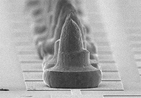
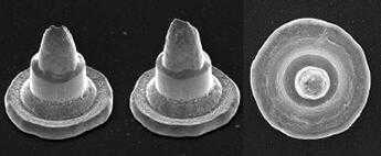
Bumping wire is a bonding wire used to form fine metal bumps (protrusions) on semiconductor chips. These bumps improve interconnection reliability in subsequent assembly processes and support high-density, high-performance packaging technologies such as flip-chip bonding and 3D packaging. Materials with high electrical conductivity, including gold and gold alloys, are commonly used.
Bumps can be formed with minimum variance in height.
Our bumping wires are available with bump formation methods for increasingly smaller, thinner, and higher-density electronics packaging. Bumps can be formed on semiconductor devices, such as ICs and LSIs, and other microelectronic devices at a lower cost and with a minimum variance in height.
Features
- Bumps can be formed with a minimum variance in neck height
- Bumps can be formed with a minimum variance in shape
- Suitable for small-volume production
Gold alloy bumping wire
GBC type
Features
- In the high temperature storage test (200℃), the shear strength after bump formation, decreases less than other bumping wires (GBC)
Gold Bumping Wire
GBE Type
Features
- Chips are not damaged during bump formation
![[Neck Height Comparison Graph]GBC/GBE/Low loop wire/Middle loop wire/High loop wire](http://files.chinaasaservice.com/8284/23257156/img_bumping_wires_02.gif)
First, please make an Inquiry about the product.
For any questions regarding product specifications, pricing, delivery times, etc., please feel free to Inquiry here.