
Precious Metals Nanoparticles
What are "Precious Metal Nanoparticles"?
These highly functional materials are made by precisely controlling precious metals such as gold and platinum at nanoscale, and exhibit a variety of properties depending on the particle structure and surface properties. Variations such as gold nanoshell particles and metal clusters are being developed, and various applications are expected in the fields of catalysis, analysis, and biology.
Precious metal nanoparticles with properties different from bulk and molecules
We design and synthesize precious metal nanoparticles with new functions not found in conventional materials, and develop new materials that can contribute to solving social issues.
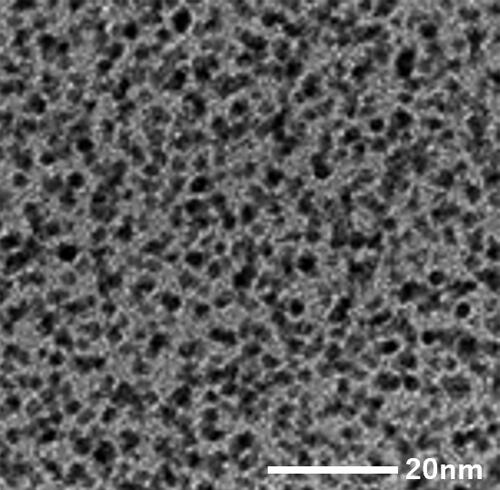
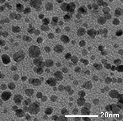
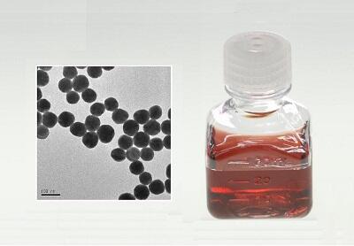
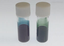
Polymer Coated Nanoparticles
Nanoparticles are generally defined as having a size between 1 and 100 nm and have unique properties that are different from both bulk metals and molecules. They are expected to be used in a variety of applications including catalysts. Nanoparticles can be stably dispersed in solvent by modifying their surface with polymers called protective agents.
Precious Metals Nanoparticles
| Product name | Precious Metals | Particle size (nm) | Protective agent | Dissipative type | ||
|---|---|---|---|---|---|---|
| Precious Metal Concentration (wt.%) |
Solvent | |||||
| Au PVP | Au | 5~10 | PVP※1 | 4 | Water | |
| Pt PVP | Pt | 2 | ||||
| Pd PVP large | Pd | 5~20 | ||||
| Pd PVP fine | 4 | |||||
| Pt PAA | Pt | 2 | PAA※2 | 2 | ||
| Pt PEI | Pt | 3~5 | PEI※3 | ~0.5 | ||
- ※1:PVP; Polyvinylpyrrolidone
- ※2:PAA; Polyacrylic Acid
- ※3:PEI; Polyethyleneimine
- We can also prototype other products upon request.
- *Mass production scale will be discussed separately.
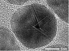
TEM image
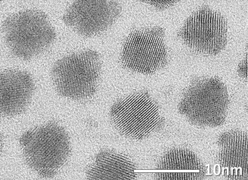
Gold Nanoshell Particles
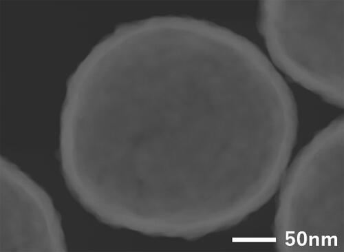
Gold nanoshell with 10 nm thickness
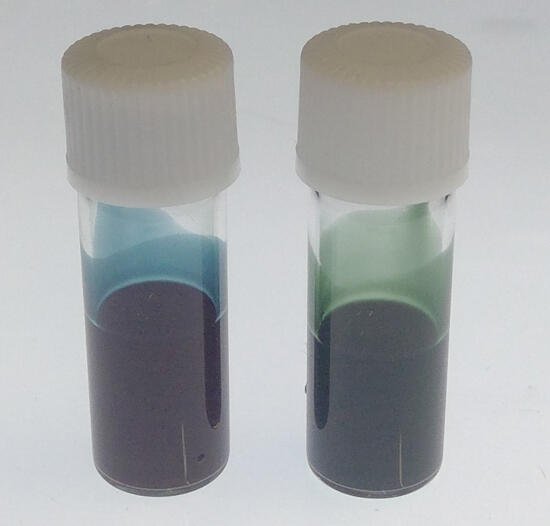
Silica nanoparticles coated with Au (gold nanoshell particles). The overall size of gold nanoshell particles can be controlled between 80 nm and 250 nm to allow a wide range of optical characteristics.
Features
- The extremely thin shell of less than 10 nm allows effective absorption of incident light energy. In addition, the specific gravity of the particles as a whole becomes lower, which contributes to stable dispersion.
- Possible to stably disperse in water and organic solvents.
- Particles protected by protective agents can be prepared with Au concentration of up to approximately 20 wt%.
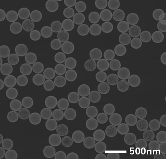
The white contrast is gold
Left: 100 nm, Right: 220 nm
This technology is expected to be used for optical materials that respond to visible light to light in the near-infrared range such as colloidal crystals, surface-enhanced Raman scattering, and photothermal conversion materials. Furthermore, it is expected to be applied in optical devices including optical displays used in LCDs that require high image quality, optical sensors, plasmonic nanoantennas, and biosensors used in cancer screening.
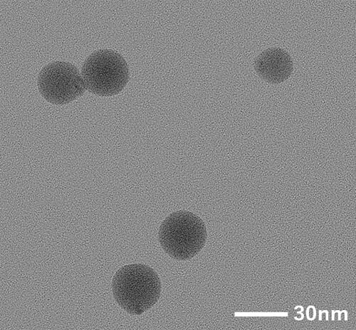
Anisotropic Precious Metal Nanoparticles
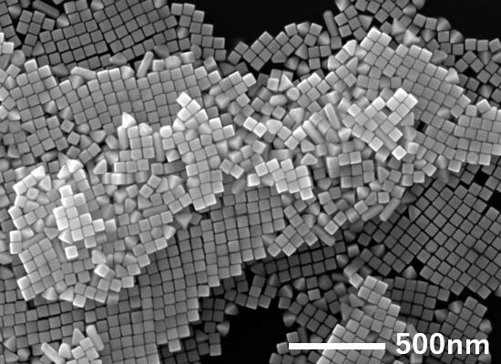
Precision-controllable gold nanocube
One side of the cube can be precisely controlled between about 20 and 100 nm. The edge shape can also be adjusted from sharp to rounded. Unlike an isotropic sphere, anisotropy occurs in the enhanced electric field due to localized surface plasmon resonance depending on the direction and angle of the incident light.
Simulation diagram of electric field enhancement of gold nanocube
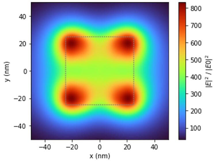
The simulation of electric field enhancement of 50 nm gold nanocube shows that when light polarized in the x-axis direction is injected, light (electric field) with an intensity hundreds of times greater than the incident light is concentrated at the edge endpoints.
Features
- In addition to cubes, other shapes such as rods and prisms can also be synthesized.
- The peak wavelength of localized surface plasmon resonance can be controlled from the visible to the infrared range by controlling the shape and size.
- Anisotropic particles can be used as a core, and other metals can be applied to the surface.
This technology is expected to be used for optical materials that respond to visible light and light in the infrared range such as for photoelectric conversion, photothermal conversion, and photocatalysis. Furthermore, it is expected to be applied to bioimaging in combination with biomolecules.
Quantum Dot
Quantum dot that can use various types of light
Semiconductor nanoparticles called quantum dot. Multi-component semiconductor nanocrystals with a uniform particle size distribution that can be produced by appropriately mixing multiple metal species and chalcogens.
Features
- The bandgap width (absorption wavelength) can be adjusted by controlling the core composition and particle size.
- A wide range of wavelengths from visible, near infrared (Near-InfraRed, NIR) to short wavelength (Short Wavelength InfraRed, SWIR) can be used.
- High-performance quantum dot can be obtained by core-shelling particles and doping specific atoms.
- Does not contain lead or other environmentally harmful substances.
- Film formation is possible using spin coating or other simple methods since ink stably dispersed in organic solvents can be produced.
This technology is expected to be applied to various fields that use light. In particular, it is expected to be used for photoelectric conversion materials such as solar cells, optical sensors, and as well as luminescent materials for laser and imaging.
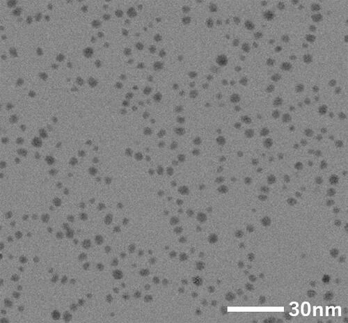
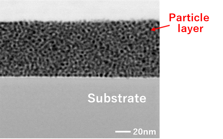
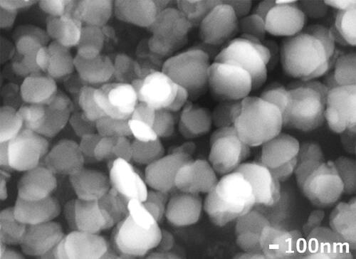
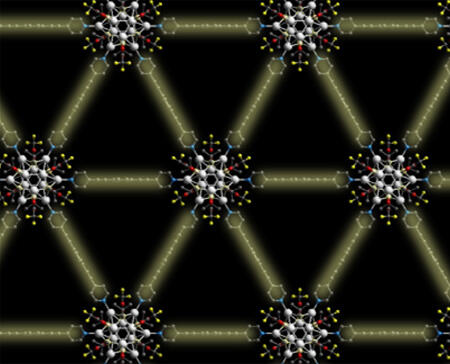
Metal Nanocluster
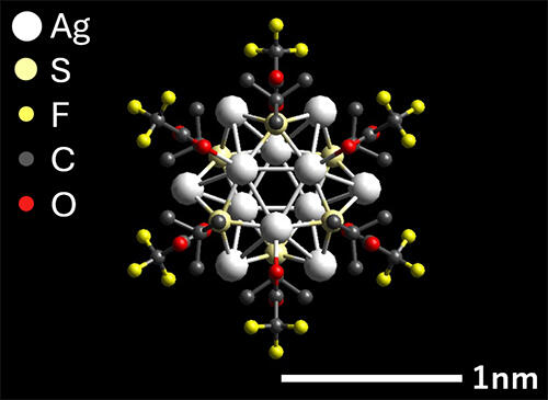
Precious metal nano cluster assembled by linker molecules
Metal nano clusters consisting of several to dozens of metal atoms bonded together are fine particles with a particle size of 4 nm or less. They are attracting attention as a constituent unit of functional nanomaterials. TANAKA is developing materials linked by organic molecules called linkers because, in general, particles become unstable as the particle size decreases.
Features
- High structural stability has been achieved through the molecular assembly using linker molecules.
- Maintaining a certain distance between clusters is expected to result in homogeneous physical properties.
- The clusters form a unique sheet structure arranged in a two-dimensional array that presents high crystallinity.
SEM image and molecular model of Ag12cluster aggregates
Related Literature:
DAS, Saikat, et al. Silver cluster-assembled materials for label-free DNA detection.
Chemical Communications, 2023, 59.27: 4000-4003.
This technology is expected to be applicable to chemical sensors, catalysts, and materials for electronic devices.
Related Information
First, please make an Inquiry about the product.
For any questions regarding product specifications, pricing, delivery times, etc., please feel free to Inquiry here.