CLOSE
About Elements
TANAKA is a leading company in the field of precious metals.
Advanced materials and solutions that support societal progress, the development stories behind them, the voices of engineers, and our management philosophy and vision—
Elements is an online media platform that shares insights that lead to a better society and a more prosperous future for the planet under the slogan “Mastering Precious Metals.”

A media platform by TANAKA
supporting societal progress with
advanced materials.


Search within Elements
Search by tags
【Considering growing emerging trends toward Photonics-Electronics Integration technologies】Unlocking the possibilities of gold: New concepts for next-generation high-density packaging
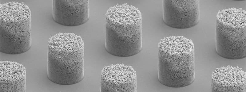
Today, in semiconductor back-end processes, the introduction of epoch-making packaging technologies is accelerating. At the same time, there is growing expectation for the development of new materials with features and properties engineered to meet the requirements of these advancing innovations. TANAKA PRECIOUS METAL TECHNOLOGIES Co., Ltd. has developed AuRoFUSE™ preform, a new mounting solution that allows high-density packaging with high reliability.
In recent years, the semiconductor and electronics fields have demanded higher communication speeds, lower power consumption, and continued device miniaturization. Technologies gaining attention to meet these demands include three-dimensional packaging, which stacks components vertically, and high-density packaging, which integrates multiple functions within a limited footprint.
One of the key elements supporting these packaging technologies is flip-chip bonding. In this method, the chip is flipped upside down onto the substrate and directly bonded, the electrodes are connected using micro-bumps. Because the bonding material must satisfy a wide range of functional requirements—including appropriate bonding temperature, as well as sufficient electrical and thermal conductivity—material selection becomes critically important.
Issues faced in materials for bump formation
Currently, soldering and plating are primarily used to form bump electrodes.
Soldering offers the advantage of low cost and fast processing, but it raises concerns regarding short-circuit risks at fine pitches. In contrast, plating is well-suited for fine-wiring structures, yet the inherent hardness of the plated material makes it difficult to absorb variations in bump height or nonuniform loading. These limitations can lead to connection failures and the generation of residual strain.
To overcome these challenges, work is currently being undertaken vigorously to develop new materials and optimize the bonding process. Further evolution of high-density flip-chip bonding technology may be the key that supports next-generation semiconductor packaging.
NEXT ≫ “Mediator” between heterogeneous chips
and substrates
This is an excerpt from an advertisement article in “Nikkei xTECH” published on November 21, 2025, reproduced with permission from Nikkei Business Publications, Inc. (Unauthorized reproduction prohibited)
Related Information
Technology Trend and Advanced Packaging Material for Power Device
Power device is key component for a wide range of applications such as smartphones, electronic devices, next-generation mobility including EV and HEV, cellular base stations, power control for renewable energy and so on. Its technology development is thriving day by day.
We introduce advanced packaging technology trends and cutting-edge materials designed to address challenges such as high heat dissipation, high heat resistance, reliable bonding in manufacturing, and miniaturization.


