
Flexible Touch Panel Sensor Using SuPR-NaP Method
TANAKA, AIST, the University of Tokyo, and Yamagata University have collaborated to develop a transparent and flexible substrate with ultra-fine wiring of just 0.8 µm.
Researchers and Developers

TANAKA PRECIOUS METAL TECHNOLOGIES
Department of Chemical Materials Development
Professor, Graduate School of Engineering, The University of Tokyo
Research Center for Flexible Electronics, AIST
Successful examples of collaboration among industry, government, and academia in Japan's microelectronics sector may become more common in the future. TANAKA PRECIOUS METAL TECHNOLOGIES from the industrial sector, the National Institute of Advanced Industrial Science and Technology (AIST) as an independent administrative institution, and Yamagata University and the University of Tokyo under the Ministry of Education, Culture, Sports, Science and Technology have joined hands to bring practical applications of flexible electronics technology closer.
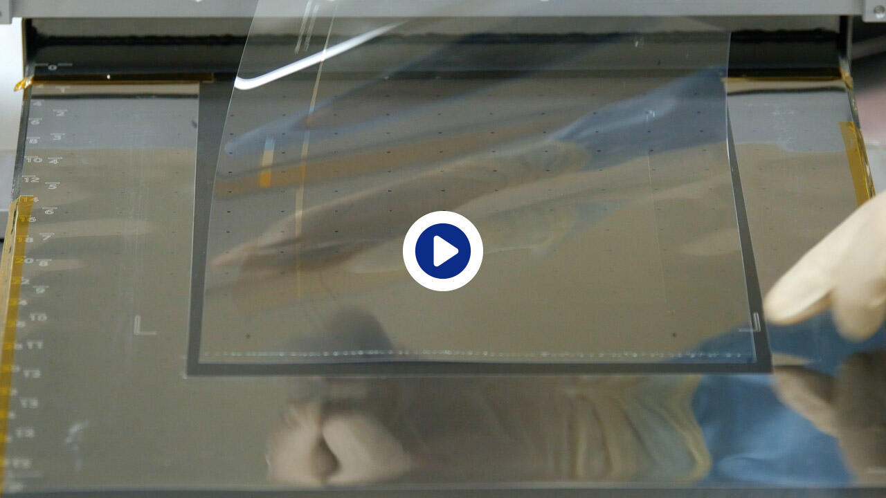
TANAKA, along with industry, academia, and government, has developed a silver wiring technology (Figure 1) with wiring widths of less than 1 µm that can be used as a transparent (conducting) electrode, and is working on commercializing the technology with the aim of starting sample shipments in January 2017.
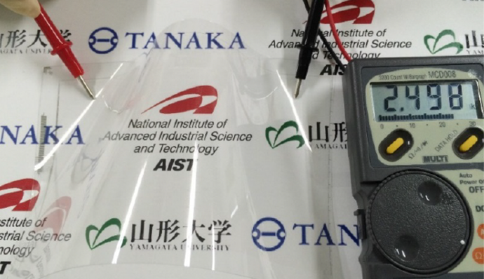
Source: National Institute of Advanced Industrial Science and Technology, The University of Tokyo, Yamagata University, TANAKA PRECIOUS METAL TECHNOLOGIES, Japan Science and Technology Agency
This is my first time using flexible wire with thin wiring.
Until now, flexible electronics have been far from practical use. The minimum wiring width that can be processed has been limited to around 30 µm at the very least. For this reason, flexible printed circuit boards (FPCs) that can be bent enough to be folded have used wiring of 100 µm or more. There have been applications for flexible substrates as a means of connecting rigid substrates. However, not many applications were expected.
In addition, rumors began circulating that organic EL would be used for the display of the iPhone 8, and organic EL has suddenly begun to attract attention over the past year or so. However, a wiring width of about 50 µm is too thick to form wiring within the pixels of organic EL displays. It must be miniaturized to a level of a few µm in order to form satisfactory organic EL displays.
If the substrate is made of thin glass, it can bend to some extent and withstand heat treatment, so lithography, a technology for processing wiring, has been used to manufacture displays. LG Electronics of South Korea has commercialized OLED TVs, while Samsung Electronics has commercialized OLED displays for smartphones. In both cases, these displays are formed on glass substrates, so they cannot be bent too much. The radius of curvature is large, ranging from several centimeters to 10 centimeters, making it difficult to manufacture smartphones that can be folded. However, if thin wiring can be formed on plastic films that can be bent with a curvature of several millimeters, such as organic polymers, the internal wiring of OLED pixels can be miniaturized.
Transistors and wiring should not be exposed to high temperatures when being formed on plastic film. Therefore, a heat treatment process at temperatures below 80°C is required. Under these adverse conditions, a technology has been developed through collaboration among industry, government, and academia that can form wiring with a minimum size of 1µm on flexible plastic film (PET resin).
FLEC by AIST and ink by TANAKA
To provide background on the development of this technology, AIST has been conducting a wide range of research and development with the aim of realizing printed electronics (a technology for forming electronic circuits using printing technology) with flexible characteristics. Among these, AIST has been utilizing surface modification technology for plastic film substrates. Tatsuaki Hasegawa, who served as Deputy Director of AIST's Center for Flexible Electronics, was developing printing technology. His appointment as a professor in the Department of Physics at the University of Tokyo's Graduate School of Engineering in January 2014 strengthened ties with the university. Meanwhile, Professor Masato Kurihara of Yamagata University's Graduate School of Science and Engineering invented and developed special ink that dissolves silver nanoparticles in organic solvents. TANAKA has been developing products using the ink developed by Yamagata University that dissolves silver nanoparticles.
The manufacturing process developed by Professor Hasegawa and this silver nanoink are key to this technology. First, let us introduce this process, called "SuperNAPP (Surface Photo Reactive Nanometal Pattering)" (Figure 2). Amorphous fluoropolymer layer is coated on a plastic film. When exposed to light, the surface of the fluoropolymer layer undergoes a chemical change and becomes a substance with high reactivity. Therefore, a mask is prepared that allows light to pass only in areas that should be thinly wired, while preventing light from passing in other areas. This is similar to the mask substrate used in photolithography, where only the patterns drawn on the mask substrate can transmit light. The light required for the surface chemical change of the polymer layer is far-ultraviolet light with a wavelength of 172 nm, which is generated by an excimer lamp filled with Xe gas.
Source: National Institute of Advanced Industrial Science and Technology, The University of Tokyo, Yamagata University, TANAKA PRECIOUS METAL TECHNOLOGIES, Japan Science and Technology Agency
After exposure, latent images with active surface patterns can be formed. Squeegee, a tool similar to a spatula, is then used to sweep ink made by dissolving silver nanoparticles in an organic solvent over it. This results in ink adhering only to the areas with surface patterns, allowing silver wiring patterns to be formed.
Protective film of silver nanoink is the key
The key to this method is the ink that only adheres to active surfaces. According to TANAKA, which is commercializing this ink developed by Professor Kurihara of Yamagata University, silver nanoparticles are spherical with a diameter of 10 to 15 nm and have a protective film on their surface. Without the protective film, the silver would stick together and would not dissolve evenly in the ink. Traditionally, films with carboxyl groups have been used as protective films. However, since carboxyl groups bond strongly with silver, heat of 250°C or higher had to be applied to remove this protective film. In AIST's SuperNUP method, the protective film on silver is expected to peel off when placed on substrates.
Therefore, a material with alkylamine groups that have weak bonding with silver was used as the protective film. The silver surface is covered with a protective film, but the alkylamine-based protective film undergoes adsorption and desorption in equilibrium, with the respective amine groups being exchanged, as stated by Hitoshi Kubo, Manager of the Chemical Materials Development Group at the Tsukuba Technical Center of TANAKA PRECIOUS METAL TECHNOLOGIES. It is said that in this quasi-stable (metastable) state, silver nanoparticles in ink can maintain this state for several months.
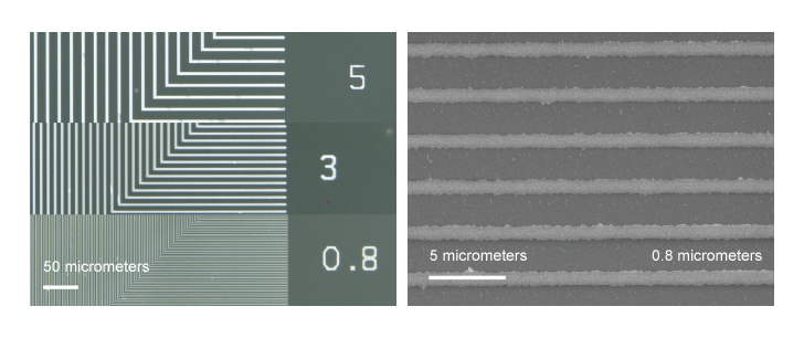
A carboxyl group is formed on the polymer active layer on the substrate surface, and when minute silver particles of 10 to 15 nm come into contact with it, the amine group peels off and the silver nanoparticles begin to bond with the carboxyl group (Figure 2). The width of the polymer active layer is almost the same as that of the mask pattern, so in the case of 1 µm width, an average of 66 to 67 silver nanoparticles with a diameter of 15 nm will be attached. Since silver also tends to bond with each other, silver nanoparticles are densely packed in the wiring bulk, and alkylamine groups are attached to the outside of the wiring. After this, heat treatment is performed at a temperature below 80 °C, during which the amine groups peel off and the wiring resistance decreases to one-tenth of that before heat treatment. So far, the company has succeeded in printing wiring for printed circuit boards with the most miniature line widths of 0.8 µm.
Source: National Institute of Advanced Industrial Science and Technology, The University of Tokyo, Yamagata University, TANAKA PRECIOUS METAL TECHNOLOGIES, Japan Science and Technology Agency
Wires are too thin and appear transparent
In general, printed circuit boards (PCBs) use copper wiring patterns instead of silver. Why was silver used? Copper is used in PCBs because it has lower electrical resistance than silver, but it has the drawback of being prone to oxidation. When copper oxidizes, its electrical resistance increases sharply. This is because oxides are insulators. Therefore, when using copper patterns or copper wires, it is necessary to carry out work in an inert gas atmosphere, such as nitrogen, to prevent oxidation. In PCBs, copper is applied to one side of a resin substrate, and a protective film is then applied to prevent oxidation. Above all, ink could not be made with copper.
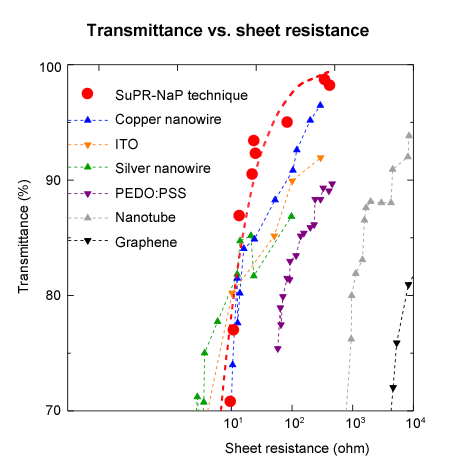
With such a fine wiring pattern as this one, visible light diffracts, causing the light waves to wrap around the back of the pattern, making it appear almost transparent. Various patterns were prepared, and the light transmittance was measured while changing their electrical resistances. The results showed that this pattern had a transparency that was comparable to the best available in the literature.
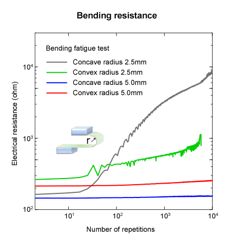
In addition, bending tests are conducted considering further applications in flexible electronics (Figure 5). At a curvature radius of 5 mm, the electrical resistance hardly changes even after 10,000 bending fatigue tests. At a radius of 2.5 mm, electrical resistance begins to rise after about 20 to 30 repetitions, which is said to be due to the underlying PET substrate starting to deteriorate. It is highly likely that this can be practically used as a flexible terminal.
However, silver wiring still has reliability issues, as dendrites are formed due to the electromigration of silver ions, which can lead to short circuits between electrodes. Therefore, it is necessary to take measures to eliminate moisture as much as possible, ensure that protective films are applied, and implement countermeasures. In this regard, TANAKA states that it has taken measures.
Source: National Institute of Advanced Industrial Science and Technology, The University of Tokyo, Yamagata University, TANAKA PRECIOUS METAL TECHNOLOGIES, Japan Science and Technology Agency
Source: National Institute of Advanced Industrial Science and Technology, The University of Tokyo, Yamagata University, TANAKA PRECIOUS METAL TECHNOLOGIES, Japan Science and Technology Agency
Aiming for Wide Applications
This technology was developed through a collaboration between AIST, the University of Tokyo, Yamagata University, and TANAKA, and was submitted to Nature Communications, accepted on December 20, 2015, and published in April 2016 (Reference 1).
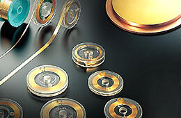
As part of its efforts toward practical application, TANAKA is developing a flexible touch panel sensor using this technology and plans to start sample shipments of the product in January 2017. Although the company has not disclosed this information, during an interview with FHE (Flexible Hybrid Electronics) Alliance Chairman Michael Ciesinski, he mentioned that ideas for flexible electronics include electronic circuits in the helmets of jet fighter pilots and rollable smartphones.
Reference Material
1. T. Yamada, K. Fukuhara, K. Matsuoka, H. Minemawari, J. Tatsumi, N. Fukuda, K. Aoshima, S. Arai, Y. Makita, H. Kubo, T. Enomoto, T. Togashi, M. Kurihara, and T. Hasegawa, "Nanoparticle chemisorption printing technique for conductive silver patterning with submicron resolution," Nature Communications, 19 April 2016.
Press Release
We introduce the potential of precious metals in various fields.

TANAKA handles everything from procurement of bullion to supply of materials, research and development, manufacturing, sales, and recycling.
We offer a full range of services related to precious metals, and by combining them optimally, we provide total solutions tailored to our customers' needs.
How was this article?
If you found this helpful, please share it.