CLOSE
About Elements
TANAKA is a leading company in the field of precious metals.
Advanced materials and solutions that support societal progress, the development stories behind them, the voices of engineers, and our management philosophy and vision—
Elements is an online media platform that shares insights that lead to a better society and a more prosperous future for the planet under the slogan “Mastering Precious Metals.”

A media platform by TANAKA
supporting societal progress with
advanced materials.


Search within Elements
Search by tags
【Considering growing emerging trends toward Photonics-Electronics Integration technologies】Unlocking the possibilities of gold: New concepts for next-generation high-density packaging
“Mediator” between heterogeneous chips and substrates
Under such circumstances regarding the use of technology in semiconductor back-end processing, TANAKA has developed AuRoFUSE preform—a new bonding solution that can achieve highly reliable, high-density flip-chip bonding—and is making preparations toward mass production and supply. This technology applies the low-temperature sintering properties of submicron-sized gold particles to produce gold bumps of various sizes and shapes (Figure 1).
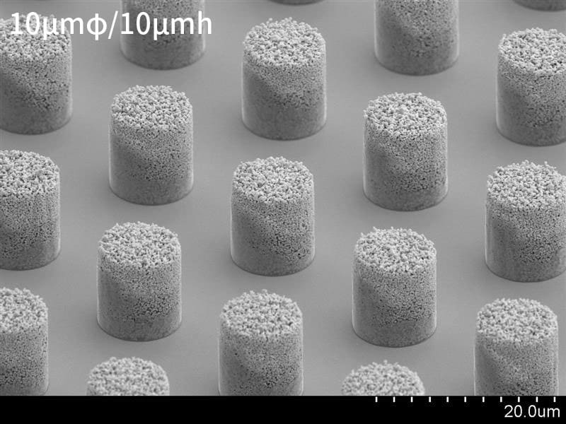
Figure 1. Gold bumps produced using AuRoFUSE preforms
Yuichi Makita, who was involved in the development, said, “The material used to connect the chip to the substrate not only needs to effectively transmit electrical signals and heat, but also needs to function as an intermediary that reconciles differences in the states and physical properties of the chip and substrate. AuRoFUSE preform is being developed as a new bonding technology that retains the advantages of wire bonding, which inherently provides both of these functions—while meeting the requirements of today’s advanced packaging landscape.”
Bumps formed using AuRoFUSE preform can undergo thermo-compression bonding at a relatively low temperature of around 200ºC. Although the connection density is slightly lower than that of hybrid bonding, the process is simpler and can reduce the mounting process load. Therefore, it can be said to be an extremely useful high-density connection technology.
After forming, the bumps have a porous structure made up of approximately 0.4 μm gold particles. Therefore, they seldom deform horizontally in size or shape when pressure is applied during connection (Figure 2). Hence, it becomes harder for short circuits to occur between electrodes, allowing high-density, highly reliable connections to be achieved. For the same reason, even if the substrate to be bonded is large and the bonding surface is uneven, the bumps can flexibly absorb warpage, unevenness, and height differences to allow high-yield mounting.
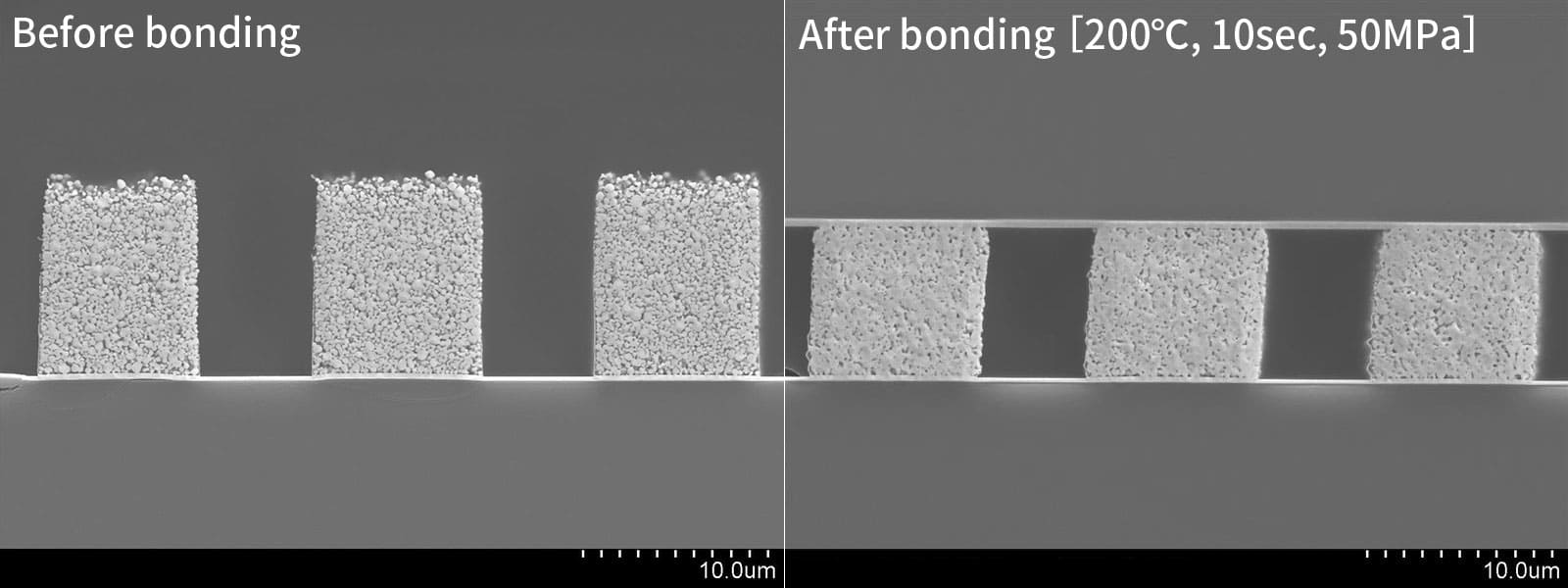
Figure 2. Dimensional changes due to compression
Like a sponge, bumps formed using AuRoFUSE can be compressed in the vertical direction with little change in size in the horizontal direction. This makes it less likely that defects such as short circuits will occur between bumps after compression.
In addition, as the main component is gold, electrical resistance is low (4.5 μΩ·cm, which can be improved by applying more pressure) and thermal conductivity is extremely high at 200 W/mK. Makita said, “It is also optimal for devices that handle large currents and generate significant heat, such as power semiconductors. Furthermore, the stable physical and chemical properties of gold suppress oxidation and migration, contributing to highly reliable long-term interconnects..”
Proposing a new process that realizes the benefits of this new material
AuRoFUSE is a paste material made of gold particles and an organic solvent. Generally, it can be dispensed using a dispenser to form bumps. However, this method is limited to forming bumps of about 600 μm.
Therefore, TANAKA developed a new process that realizes the benefits of AuRoFUSE, making it possible to form tiny, high-density gold bumps with a minimum size of 5 μm and spacing of 5 μm (Figure 3). Comprising a combination of the photolithography process with the paste printing process, the gold bump formation process that was developed is highly compatible with existing processes.
Figure 3. Gold bump formation process
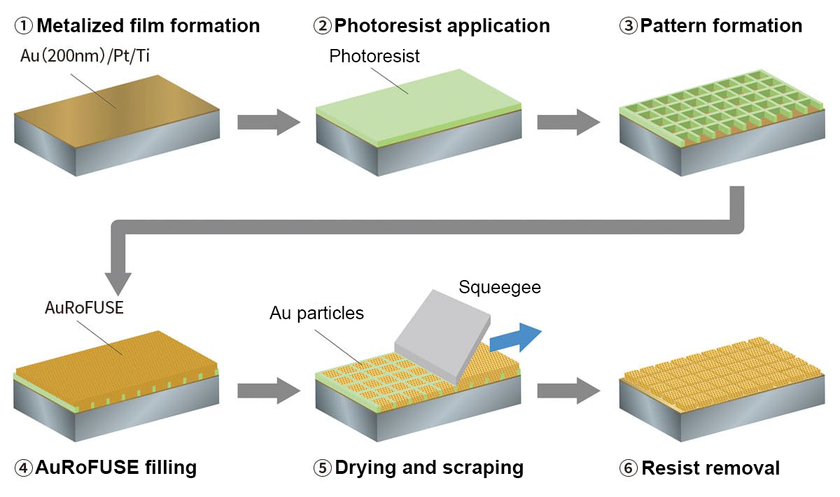
First, a thin metal film (Au/Pt/Ti) is formed on the bonding substrate to create the base layer. Then, photoresist is applied, and the bump pattern is formed using an exposure process. After the paste is filled through printing, resist stripping and drying are performed to produce the preforms.
TANAKA does not only supply materials but is also working on the development of a support system so that our user can implement the gold bump formation process as a mass-production process. A system will be established to recycle used materials, achieving both sustainable use and reduced costs for users, as the technology uses gold, a precious metal with excellent functionality.
Naoto Watanabe, who is working to develop application markets, said, “We are proud that AuRoFUSE preform is a technology that could only be achieved at TANAKA, which has been honing and developing technologies in precious metals for 140 years. Currently, we are studying further improvement of performance and expansion of application scope. In particular, it is expected to be applied to thermally demanding applications such as micro-LEDs and photonics-electronics integration chips.”
Semiconductor chips will likely achieve further evolution through the use of next generation mounting solutions such as AuRoFUSE preform.
This is an excerpt from an advertisement article in “Nikkei xTECH” published on November 21, 2025, reproduced with permission from Nikkei Business Publications, Inc. (Unauthorized reproduction prohibited)
Related Information
Technology Trend and Advanced Packaging Material for Power Device
Power device is key component for a wide range of applications such as smartphones, electronic devices, next-generation mobility including EV and HEV, cellular base stations, power control for renewable energy and so on. Its technology development is thriving day by day.
We introduce advanced packaging technology trends and cutting-edge materials designed to address challenges such as high heat dissipation, high heat resistance, reliable bonding in manufacturing, and miniaturization.


