
Improving the Reliability of Precious Metal Brazing Filler Metals in Power Devices

Monthly "Welding Technology" June 2022 issue
TANAKA PRECIOUS METAL TECHNOLOGIES CO., LTD.
1. Introduction
Power devices are semiconductor devices that convert electrical power and are used in many applications, including automobiles, renewable energy, and industrial equipment. In particular, in automotive applications, hybridization and electrification are being promoted, and the demand for power devices is increasing year by year. In terms of performance, development is also underway for higher efficiency, smaller size, and higher output, and for the various components that make up power devices, improvements in performance and reliability that can withstand more demanding operating environments are required.
Figure 1 shows the structure of a power device. A power device is made up of multiple components, and these components are made of various materials such as semiconductors, metals, and ceramics. The components are bonded together, and the bonding of different types of materials occurs at multiple interfaces. When a power device is not in operation, for example, while a vehicle is parked, it is cooled to a temperature close to the outside air temperature. In particular, during winter, it may be cooled to below freezing, and in some regions, it may be cooled to several tens of degrees below zero. On the other hand, when the vehicle starts to move, electricity flows through the power device, causing it to generate heat, and the temperature rises to over 100°C. In this way, each time the power device is operated, heating and cooling are repeated, and the components that make up the power device and their bonding parts undergo repeated thermal shock, with particularly significant stress occurring at the bonding parts of different types of materials.

Among the components that make up power devices, there is one called ceramic circuit board. It has a structure in which copper plates are bonded to both sides of a ceramic plate, with the surface having the function of an electric circuit and the reverse side serving as a heat dissipation. The ceramic plate positioned in the center has an important role in insulating electrically between this electric circuit and the cooling device while allowing the heat generated by the semiconductor device to escape to the cooling device. The copper bonded to the surface of the ceramic plate expands significantly due to the heat generated by the operation of the power device, and when the operation ends, it cools and contracts. On the other hand, ceramics have a property that they hardly expand due to heat. For this reason, in ceramic circuit boards, only copper expands and contracts repeatedly due to temperature changes, and stress due to expansion and contraction generated by temperature changes is repeatedly applied to the bonding interface with ceramics. Furthermore, until now, the operating temperature of power devices was considered to be a maximum of about 150°C, but in the future, there will be demands for operation at even higher temperatures of 175°C and 200°C1), and the requirements for the thermal shock durability and reliability of ceramic circuit boards are increasing day by day. In addition, until now, it has been common to use copper plates with a thickness of about 0.3 mm bonded to ceramic plates, but there are also attempts to use copper with a thickness of 0.8 mm or more to improve heat dissipation performance, and the performance required of ceramic circuit boards is increasing day by day.
This report discusses the reliability of ceramic circuit substrates, one of the components of power devices.
2. Background and Purpose of Application
There are several methods for bonding ceramic substrates and copper used in ceramic circuit substrates, one of which is bonding by brazing.
Brazing is generally a bonding method used for joining metals, and ceramics cannot be joined using brazing. However, it is possible to directly braze ceramics using a special type of brazing filler metal known as active brazing filler metal. Active metal is a type of brazing filler metal that has improved wettability on ceramics by adding titanium or other active metals as an alloying element. Active brazing filler metals with silver and copper are well known and are also used in the manufacture of ceramic circuit substrates.
A typical method for manufacturing ceramic circuit substrates is shown in Figure 2. First, active brazing filler metal used for bonding is in paste form. This paste brazing filler metal is produced by mixing metal powders of silver, copper, and titanium with an organic solvent. This brazing filler metal paste is applied to a ceramic plate such as silicon nitride, and a copper plate is placed on top of it. Heating is then performed in a vacuum to melt the brazing filler metal paste and carry out brazing. At this time, if an eutectic alloy of silver and copper is used, the melting point is 780°C, so brazing can be performed at a temperature of around 800°C. However, since the brazing filler metal paste used in this method is in a state where, as mentioned earlier, the powders of silver, copper, and titanium are mixed, it does not melt at 800°C heating, and brazing is performed by heating to 900°C or higher, close to the melting point of silver.
After brazing, copper is bonded to both sides of the ceramics, but since a circuit pattern needs to be formed on one side, copper on that side is removed by etching. Masking is performed on the surface of copper to form a circuit pattern, and copper is etched using an etching solution. Furthermore, after etching copper, a brazing material layer remains, so the brazing material layer is also etched to form a circuit pattern. After going through the above processes, the ceramic circuit substrate is completed.

Ceramic circuit substrates are manufactured through processes like this, but there are some concerns regarding reliability when this method is used. One is the impact of high soldering temperatures (above 900°C). The second is damage to the ceramics caused by etching.
First, regarding the high brazing temperature, ceramics generally have a lower thermal expansion rate than metals. When brazing is performed at high temperatures and then cooled, significant residual stress occurs at the bonding interface due to the difference in thermal expansion coefficients between ceramics and metals. As mentioned at the beginning of this paper, each time a power device operates, repeated thermal shock is further applied from this state. However, since significant stress is already present after brazing, it is desirable to lower the brazing temperature as much as possible to suppress the expansion of copper and minimize the stress generated at the bonding interface with ceramics.
Next, regarding damage from etching, ceramics and copper are joined with a brazing filler metal layer, and a titanium compound layer formed by the reaction between titanium contained in active brazing filler metal and the components of ceramics is present at the interface between the brazing filler metal layer and ceramics. If the brazing filler metal layer and titanium compound layer remain on the surface of ceramics, insulation between circuit patterns cannot be ensured, which poses a risk of electricity flowing to unexpected locations. Therefore, they must be completely removed. Currently, ammonium fluoride and other substances are used for the removal of titanium compounds. However, this method may remove titanium compounds while also damaging the ceramic substrate and silicon nitride, raising concerns about reduced reliability.
As described above, conventional methods have several concerns, which are expected to become issues when higher durability and reliability are required in the future. Therefore, it is necessary to develop a new method for manufacturing ceramic circuit substrates that can solve these problems.
3. Description of Technology
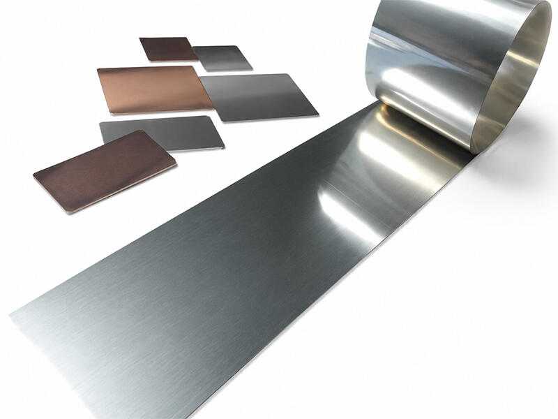
To solve the issues mentioned above, we considered a method for manufacturing ceramic circuit substrates that allows for lower brazing temperatures and does not require an etching process. As a solution, we considered using active brazing filler metal/copper clad material, which is clad with active brazing filler metal and copper. The details are provided below. A photograph of active brazing filler metal/copper clad material is shown in Figure 3. It has a structure in which a thin layer of active brazing filler metal is attached to one side of copper. The material was manufactured by continuously bonding copper and active brazing filler metal, followed by punching using press processing. The thickness of the copper is 0.8 mm and the thickness of the filler metal is 20 µm.

The brazing filler metal used for this composite material is AgCuSnTi alloy. As mentioned earlier, active brazing filler metals are known to be composed of silver, copper, and titanium, and brazing filler metal of AgCuTi alloy is also available on the market. However, when AgCuTi alloy is melted and cast, then processed into a plate form in order to obtain foil, as shown in Figure 4, coarse CuTi compounds appear in the metal structure. This coarse compound is very hard, and as processing continues, it can protrude from the surface of the rolled material or fall off the material, leading to breakage and pinholes in the rolled material, making it difficult to process into thin sheets and foils. Naturally, it was also impossible to bond with copper.

As a result, we have previously considered whether it is possible to improve the microstructure of AgCuTi alloys by adding other materials. We found that by using AgCuSnTi alloy, titanium compounds can be finely dispersed. Based on this, we have developed an active brazing filler metal using AgCuSnTi alloy. This time, we were able to prototype the above clad material using this AgCuSnTi alloy.
Figure 5 shows the manufacturing process for ceramic circuit boards using active metal brazing filler copper clad material. The active metal brazing filler copper clad material is pressed into the desired shape, such as the circuit or heat sink, and placed on a ceramic plate. Positioning can be achieved using a carbon jig or similar tool. The brazing process is then performed by heating in a vacuum furnace. The melting point of the brazing filler metal used in this study is approximately 750°C. Because the brazing filler metal is an alloy, it can be brazed at 800°C, eliminating the need for heating above 900°C as with the paste mentioned above. Furthermore, since the desired shape is already achieved by pressing, no etching process is required after brazing, eliminating the risk of damage to the ceramic due to the etching process. Thus, we believe that the new manufacturing process using active metal brazing filler copper clad material overcomes the concerns of the conventional method mentioned above.

4. Past Achievements
Figure 6 shows a sample of a ceramic circuit substrate on which actual brazing was performed using active brazing filler metal and copper-clad material.

The dimensions used were 0.8 × 30 × 30 mm for the composite material (with a 20 µm thick solder layer) and 0.32 mm thick for the silicon nitride.
Figure 7 shows the results of an observation of the interface after bonding. Observations were performed using a transmission electron microscope (TEM). TEM observations confirmed that titanium was concentrated near the ceramic, and that this titanium layer was uniformly distributed across the entire bonded interface. The titanium layer, starting from the side closest to the silicon nitride, was TiN-Ti5Si3. These compounds are generally formed when silicon nitride is bonded with an active metal brazing filler metal.2) We believe that the brazing occurred due to a reaction between the AgCuSnTi alloy active metal brazing filler metal and the silicon nitride. Furthermore, when nitride-based ceramics are bonded with an active metal brazing filler metal, the formation of an excessive TiSi layer at the interface between the ceramic and brazing filler metal has been reported to result in a decrease in strength.3) In this case, the TiNi layer was present across the entire bonded interface, but the Ti5Si3 layer was only partially formed and discontinuous. This does not present a risk of forming an embrittlement layer that adversely affects bond reliability, and we believe that a good bond was obtained.

Next, thermal cycle tests were conducted to evaluate reliability. Thermal cycle test is one of the evaluation tests that simulate the operation of power devices. In this test, the sample is subjected to thermal shock by alternately moving between a cooling chamber and a heating chamber, and its durability against thermal shock is evaluated. In this test, the cooling chamber was set to -50°C and the heating chamber to 175°C, with a holding time of 30 minutes each and a cycle time of 1 hour. The evaluation method used was ultrasonic flaw detection to measure and evaluate the condition after soldering and the condition after every 250 cycles of thermal cycle tests.
Thermal cycle test results are shown in Figure 8.

No voids or peeling were observed immediately after brazing or before thermal cycle testing, and it was confirmed that copper and ceramics were bonded over the entire surface. Furthermore, even as the tests progressed through 250 and 500 cycles, there were no changes in this state, and no changes were observed even after 1,500 cycles. Therefore, it was confirmed that ceramics substrates produced using the active metal brazing filler metal have sufficient durability against thermal shock, and are considered to have high reliability against thermal shock.
5. Future Developments
To ensure even higher reliability, we believe that further lowering the brazing temperature could be one solution. We are currently optimizing brazing filler metal components to lower the brazing temperature. In addition, we anticipate that power devices will become even smaller and that their power density will increase, so we believe that it will also be necessary to improve heat dissipation. As a solution, we are also considering a double-sided cooling structure. Figure 9 shows an example of its application. In this structure, heat generated by semiconductor devices, which was conventionally dissipated only in the downward direction, can now be dissipated in both upward and downward directions by placing ceramic circuit substrates on both sides, thereby improving heat dissipation performance. In this case, we are considering a method of simultaneously forming terminals with circuit patterns on the surface of the ceramic circuit substrate. Since active metal brazing filler metal/copper clad materials can be easily manufactured in this shape, we believe that this shape can be easily produced and that the characteristics of active metal brazing filler metal/copper clad materials can be utilized.

6. Conclusion
Ceramic circuit substrates, which are components of power devices, are manufactured using conventional methods. However, there are concerns that reliability may decrease due to damage to ceramics from soldering at high temperatures and from chemical solutions during the etching process, and that they may not be able to cope with the more severe operating environments that are expected in the future.
To address this issue, we have developed active brazing filler metal and copper clad material to lower brazing temperatures and are considering methods that do not require etching.
Soldering temperature can be reduced from the conventional 900℃ or higher to 800℃, a reduction of 100℃. By performing press working before soldering to form the circuit pattern, a process that does not require an etching process can be used. For a sample of ceramic circuit substrate manufactured using this new method, evaluation results from thermal cycle tests showed that it has a durability of over 1,500 cycles under the conditions of -50℃ to 175℃, and it is believed that this ceramic circuit substrate can be manufactured with high reliability that can withstand the requirements for the usage conditions expected in the future under harsh environments.
The Company plans to continue developing various technologies, including optimizing active brazing filler metal components and applying clad materials, to further lower brazing temperatures and achieve better heat dissipation through double-sided cooling. Through these technologies, we hope to enhance the reliability of power devices, enable more efficient energy use, and contribute to a better future for the Earth.
References
1)Supervised by: Katsuaki Suganuma Elemental Technologies and Reliability for Next-Generation Power Semiconductor Packaging
2) Shichiyou et al.: Journal of the Ceramic Society of Japan 97 [11] 1354-57 (1989)
3) K. Nagatsuka et al.: Proceedings of the Japan Welding Society, Vol. 31, No. 1, pp. 16-22 (2013)
Related Information
How was this article?
If you found this helpful, please share it.