
【With a focus on potential use in photonic fusion, which is attracting attention】"Gold" opens up new ideas for next-generation high-density mounting
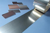
Currently, in semiconductor back-end processes, the introduction of new technologies that are expected to be epoch-making, particularly packaging technologies, is accelerating. At the same time, there are rising expectations for the creation of materials with new characteristics and properties based on new ideas in response to this innovation. TANAKA PRECIOUS METAL TECHNOLOGIES has developed a new mounting solution, "AuRoFUSE™ Preform," that has high reliability and enables high-density mounting.
In recent years, the semiconductor and electronic device sectors have been demanding faster communication speeds, reduced energy consumption, and further miniaturization of devices. Among the technologies that are attracting attention in response to these needs are 3D mounting, which stacks components in the height direction, and high-density mounting, which packs multiple functions into a limited space.
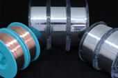
One of the key elements supporting these mounting technologies is flip chip bonding. In this method, chips are flipped over and directly bonded to substrates, with the electrode parts connected by microbumps. Since bonding materials require various functional characteristics, such as bonding temperature and electrical and thermal conductivity, material selection is extremely important.
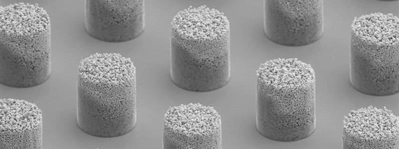
Challenges Facing Bump Formation Materials
Currently, bump electrodes are mainly formed using solder or plating.
Solder has the advantage of low cost and rapid processing, but there are concerns about the risk of short circuits at narrow pitches. On the other hand, plating has excellent compatibility with fine wiring, but its material hardness can be detrimental, leading to issues such as variations in height and uneven load that it cannot absorb. This can result in problems such as poor connections and residual strain.
To overcome these challenges, the development of new materials and the optimization of bonding processes are currently being actively pursued. The further evolution of flip chip technology is expected to be the key to supporting the next generation of semiconductor packaging.
NEXT ≫ The "mediator" between heterogeneous chips and substrates
This is an excerpt from an advertising article published in "Nikkei Crosstech" (published on November 21, 2025) with permission from Nikkei BP.
(Reproduction without permission prohibited)
Related Information
Latest Trends in Power Semiconductor Packaging Technology and Cutting-Edge Materials for High Heat Dissipation and High Heat Resistance
As energy-saving technologies for smartphones and electronic devices, next-generation mobility such as electric vehicles, base stations, and power control for renewable energy continue to advance, the technological development of power semiconductors will increasingly focus on higher output and efficiency.
We will introduce cutting-edge materials to address challenges such as high heat dissipation, high heat resistance, bonding reliability, and miniaturization, as well as trends in packaging technology.


How was this article?
If you found this helpful, please share it.