
【With a focus on potential use in photonic fusion, which is attracting attention】"Gold" opens up new ideas for next-generation high-density mounting
“Adjuster” between different chips & substrates
TANAKA PRECIOUS METAL TECHNOLOGIES is developing a new mounting solution, "AuRoFUSE Preform," that can achieve highly reliable and high-density flip chip mounting against the backdrop of the technology's use in semiconductor back-end processes. This solution is being prepared for mass production and commercialization. This technology uses the low-temperature sintering properties of submicron-sized gold particles to produce gold bumps of various sizes and shapes (Figure 1).
Yuichi Makita, who was involved in the development, said, "The material used to connect the chip to the board not only needs to effectively transmit electrical signals and heat, but also needs to act as an 'adjuster' to reconcile the differences in the state and physical properties of the chip and board. AuRoFUSE preform inherits the functions of wire bonding, which has both of these characteristics, and we are developing it as a new connection technology that meets the needs of the times."
Bumps formed using AuRoFUSE preforms can be thermocompression-bonded at around 200°C, a relatively low temperature. Although this method has slightly lower connection density than hybrid bonding, it is a highly useful high-density connection technology as the process is simpler and the burden on the mounting process can be reduced.
After formation, the bump has a porous structure made of gold microparticles of about 0.4 μm, so it is less likely to have its size and shape distorted in the width direction due to pressure during connection (Figure 2). This makes it unlikely for short circuits to occur between electrodes, enabling high-density and highly reliable connections. For similar reasons, even when the substrate to be bonded is large and the bonding surface is uneven, warping, unevenness, and step differences can be flexibly absorbed, allowing mounting with high yield.
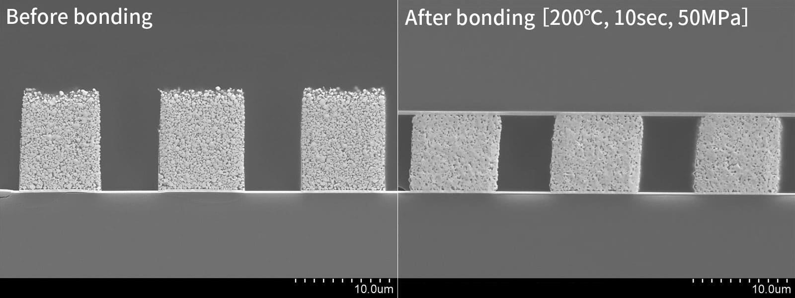
Bumps formed using AuRoFUSE have minimal size changes in the width direction, similar to a sponge, and can be compressed in the height direction. As a result, defects such as short circuits between bumps after compression are unlikely to occur.
In addition, since gold is the main component, it has low electrical resistance (4.5 μΩ・cm, which can be improved by applying pressure) and extremely high thermal conductivity of 200 W/mK. “This makes it ideal for mounting on devices that handle large electric currents, such as power semiconductors, which generate significant heat. Furthermore, due to the stable physical properties of gold, oxidation and migration are unlikely to occur, ensuring highly reliable bonding over the long term,” says Makita.
Proposing new processes that harness the power of new materials
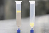
AuRoFUSE is a paste material composed of gold microparticles and organic solvents. It can generally be used to form bumps by being extruded from a dispenser. However, with this method, the formation of bumps is limited to around 600 μm.
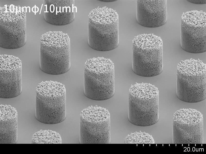
The Company has therefore developed a new process that leverages the benefits of AuRoFUSE, enabling the formation of miniature and high-density gold bumps with a minimum size of 5 μm and a 5 μm pitch (Figure 3). The developed gold bump formation process is constructed by combining a paste printing process with the photolithography process, and has a high degree of compatibility with existing processes.
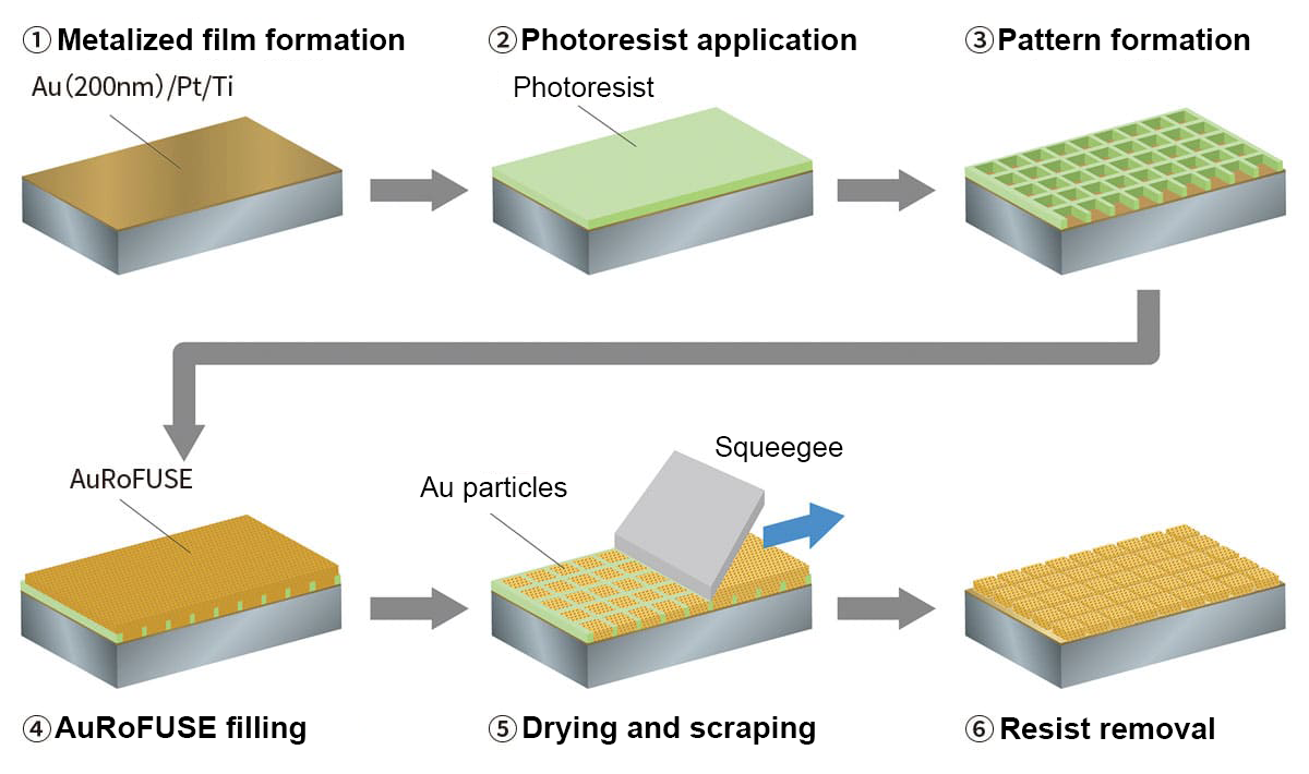
First, a metal thin film (Au/Pt/Ti) that serves as the base for connections is deposited on the substrate, and then photoresist is applied to form a bump pattern during the exposure process. After that, paste is embedded by printing, the resist is removed, and the product is dried to form a preform.
The Company is also working on establishing a support system to assist user companies in launching the gold bump formation process as a mass production process, in addition to supplying materials. Since this technology uses gold, a precious metal with excellent functionality, the Company will establish a system for recycling used materials to ensure their sustainable use and reduce costs for users.
"We take pride in AuRoFUSE preforms as a technology that can only be realized by our company, which has been refining and accumulating technologies related to precious metals for 140 years. We are currently considering further performance improvements and expanding the range of applications, and we expect this technology to be applied in areas where heat control is critical, particularly as a light source for microLEDs and optoelectronic fusion chips," says Naoto Watanabe, who is involved in developing new applications.
With the use of new era mounting solutions such as AuRoFUSE preforms, semiconductor chips are expected to further evolve.
This is an excerpt from an advertising article published in "Nikkei Crosstech" (published on November 21, 2025) with permission from Nikkei BP.
(Reproduction without permission prohibited)
Related Information
Latest Trends in Power Semiconductor Packaging Technology and Cutting-Edge Materials for High Heat Dissipation and High Heat Resistance
As energy-saving technologies for smartphones and electronic devices, next-generation mobility such as electric vehicles, base stations, and power control for renewable energy continue to advance, the technological development of power semiconductors will increasingly focus on higher output and efficiency.
We will introduce cutting-edge materials to address challenges such as high heat dissipation, high heat resistance, bonding reliability, and miniaturization, as well as trends in packaging technology.

How was this article?
If you found this helpful, please share it.