
EDITOR`S PICKS: TANAKA Establishes Transfer Technology for its Sintered Gold Bonding Technology
Source: Semiconductor Digest
Date: February 03, 2026
Author: Pete Singer, Co-Founder/Editor-in-Chief, SEMICONDUCTOR DIGEST
Link: TANAKA Establishes Transfer Technology for its Sintered Gold Bonding Technology - Semiconductor Digest
EDITOR`S PICKS: TANAKA Establishes Transfer Technology for its Sintered Gold Bonding Technology
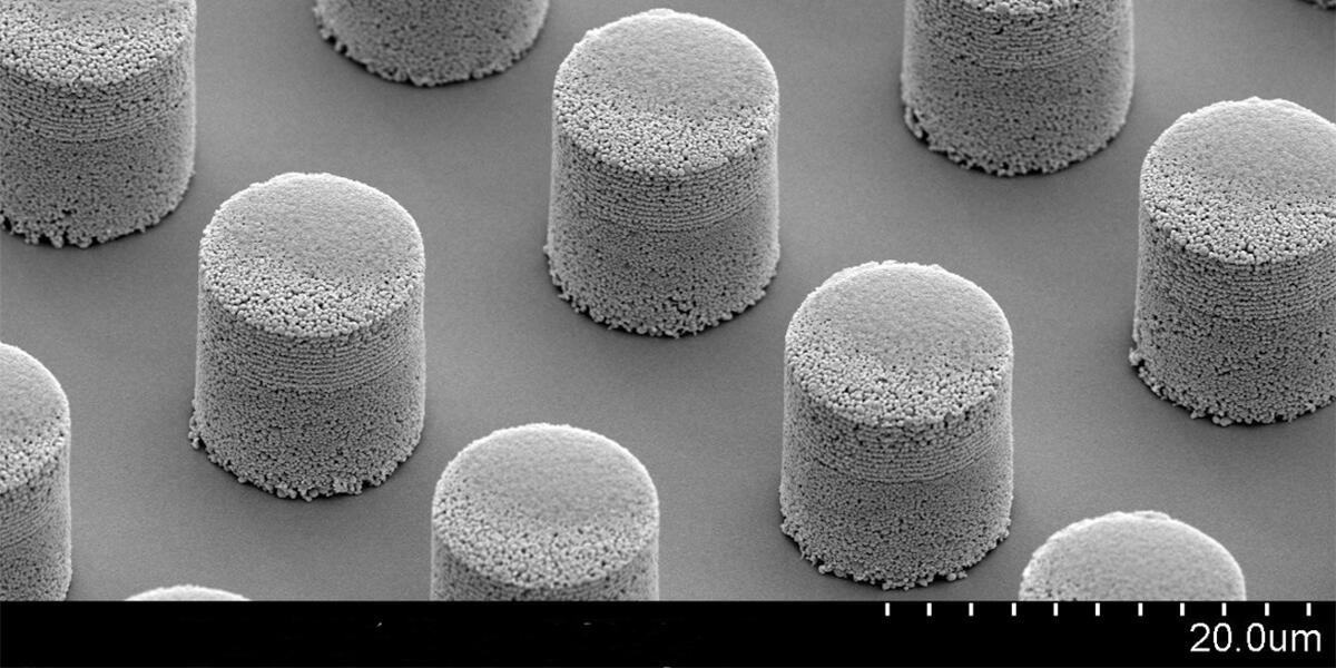
TANAKA PRECIOUS METAL TECHNOLOGIES Co., Ltd., a company engaged in the industrial precious metals business of TANAKA, today announced a gold bump transfer technology for the sintered gold (Au) bonding technology “AuRoFUSE™ Preforms.” This technology allows AuRoFUSE™ Preforms (gold bumps) to be formed even on semiconductor chips and substrates with complex structures.
Advantages of being able to transfer gold bumps
In this technology, at first, gold bumps are formed on a substrate (transfer substrate). Then, the gold bumps are transferred to the target semiconductor chip or substrate. Openings are created on the silicon substrate used as the transfer substrate, and gold bumps are formed in them. By filling the entire opening, the gold bump is held by the substrate, eliminating the risk of dropping during the process. Meanwhile, during transfer, the gold bump shrinks under heat-treatment, forming a tiny gap between the opening and the gold bump. This allows easy extraction of gold bumps by the application of a force in the vertical direction.
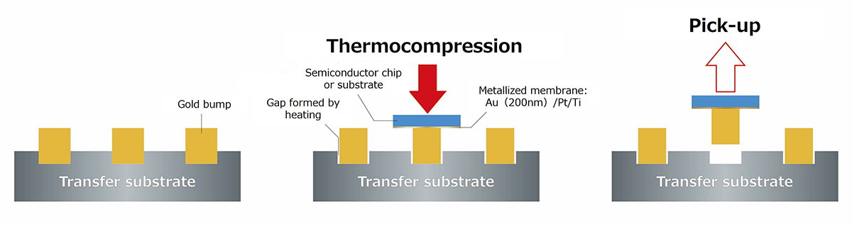
As the traditional gold bump formation process is a method that directly forms bumps on the target semiconductor chip or substrate, it is difficult to handle target chips and substrates with complex shapes, such as protrusions, dents, or open holes due to issues such as inconsistent resist heights.
In this current transfer technology, gold bumps are manufactured separately and can be transferred only to the target locations. This allows the technology to also be applied to complex shapes. It can also be used with semiconductor chips and substrates that are difficult to process using photolithography due to concerns about damage from stripping solutions and others.
This article was reprinted from an article published in “SEMICONDUCTOR DIGEST” on March 03, 2026, with permission from SEMICONDUCTOR DIGEST. This article was translated by TANAKA from SEMICONDUCTOR DIGEST with their permission.
This article was published on SEMICONDUCTOR DIGEST. Further information can be found here:
Learn more… (Semiconductor Digest)
Related Information


Technology Trend and Advanced Packaging Material for Power Device
Power device is key component for a wide range of applications such as smartphones, electronic devices, next-generation mobility including EV and HEV, cellular base stations, power control for renewable energy and so on. Its technology development is thriving day by day.
We introduce advanced packaging technology trends and cutting-edge materials designed to address challenges such as high heat dissipation, high heat resistance, reliable bonding in manufacturing, and miniaturization.
How was this article?
If you found this helpful, please share it.