
Sintered Gold(Au) Bonding Technology: AuRoFUSE™ Preform
What is "AuRoFUSE™ Preform"?
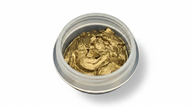
This is an Au sintering bonding technology for high-density packaging that utilizes AuRoFUSE™, a low-temperature sintering paste for gold-gold bonding developed by TANAKA. It contributes to efficient packaging processes and high reliability of bonding, and has high-performance properties such as electrical resistance of 4.5µΩ·cm and thermal conductivity of 200W/m·K.
Technical Information on AuRoFUSE™ Preforms
Sintered Au bonding technology for high-density mounting using AuRoFUSE™
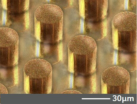
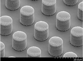
In this technology, the bonding material is dried prior to bonding to eliminate fluidity, which suppresses creeping and minimizes spreading in the horizontal direction, thereby allowing fine-pitch bonding. So far, bumps of 5 µm have been successfully formed, and this technology is expected to be used as a bonding technology for flip-chip bonding that require high-density mounting.
Features
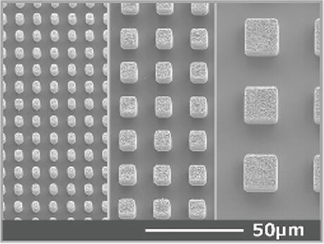
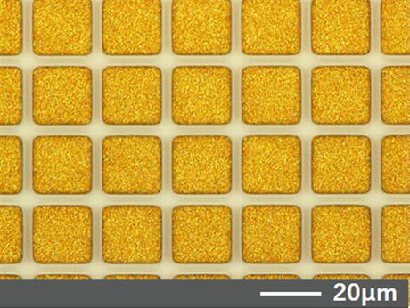
- ①Can produce gold bumps of various sizes and shapes
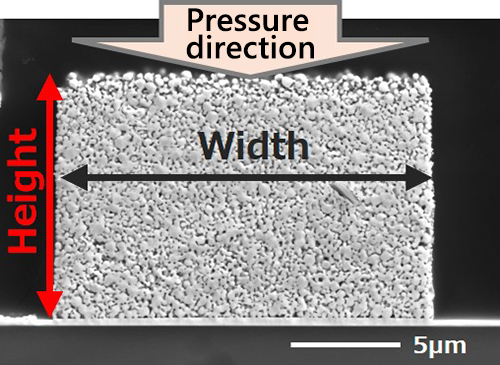
(Minimum size: 5 µm size, 5 µm pitch) - ② Has excellent compression deformability as it is a bonding material with porous structure
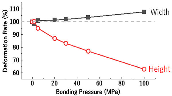
- ③ High-density mounting is possible due to minimal deformation in the horizontal direction during compression
- ④ Oxidation and migration are unlikely as the main component is Au
- ⑤ Bonding is possible at comparatively low temperatures (from 200℃) and air atmosphere

③ Shape Deformation rate when bonding pressure is increased
Expected applications
Die-bonding materials for optical semiconductors (LED and LD), power semiconductors, ICs
Manufacturing of AuRoFUSE™ Preforms
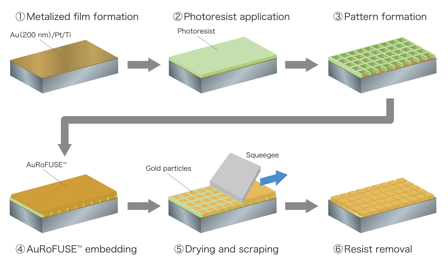
- ① Perform metallization using Au/Pt/Ti as a base layer on the substrate to be bonded
- ② Apply photoresist to the substrate for bonding after metallization
- ③ Place a photomask that matches the preform shape over the substrate to be bonded, and perform exposure and development to create a resist frame.
- ④ Flowing of AuRoFUSE™ into the formed resist frame
- ⑤ Vacuum-dry at room temperature, and after drying, scrape off excess Au particles with a squeegee.
- ⑥ Temporary sintering through heating, followed by separation and removal of the resist frame
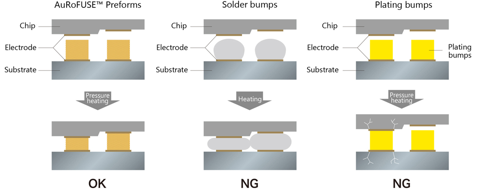
Comparison of AuRoFUSE™ Preforms and Other Materials
(〇) AuRoFUSE™ Preforms
- Drying the paste before bonding to eliminate fluidity can suppress lateral spreading and enable high-density mounting.
- Being a porous structure, it can be easily deformed, allowing bonding even when there are differences in height between electrodes, warpage of substrates, and differences in thickness.
(△) Soldering materials
- As bump pitch becomes finer, solder materials spread laterally when melted, which can cause a short circuit due to contact between electrodes.
(△) Electroless plating
- Can achieve narrow pitch, but requires relatively high pressure during bonding, which can lead to chip damage
Example of bonding: Flip-chip bonding
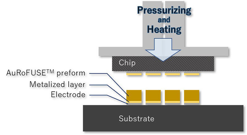
| Pretreatment: | UV ozonation, etc. |
| Thermo-Compression: | 200℃, 20MPa, 10sec. |
| Post-Bake: | 200℃, 60min. |
Characteristics
| 200℃, 20MPa, 10sec | 200℃, 100MPa, 10sec | |
|---|---|---|
| Electrical resistivity (µΩ·cm) | 3.0 | 2.6 |
| Thermal conductivity (W/mK) | 250 | 280 |
| Young's modulus (GPa) | 57 | 70 |
| Coefficient of Liner Thermal Expansion (CTE) (ppm/K) | 14 | 14 |
| Shear strength (MPa) | >30 | |
| Under Barrier Metal | Au/Pt/Ti, Au/Pd/Ni | |
AuRoFUSE™ Preforms Transfer Technology
This method involves creating a substrate with bumps formed in advance and then transferring the bumps from that substrate to the target chip or substrate.
Since bumps are formed and held in the openings of the substrate, there is no risk of bumps falling off during transport.
During transfer, bumps shrink due to heating, so they can be easily pulled out by applying only vertical force.
■ Features
- ① Can be applied to semiconductor chips and substrates with shapes that are difficult to handle using conventional methods, such as uneven surfaces and through holes
- ② Can be used for semiconductor chips and substrates that are not easily subjected to photolithography due to concerns about damage from stripping solutions and other sources
■【Fabrication of Transfer Substrates and Transfer and Bonding Processes】
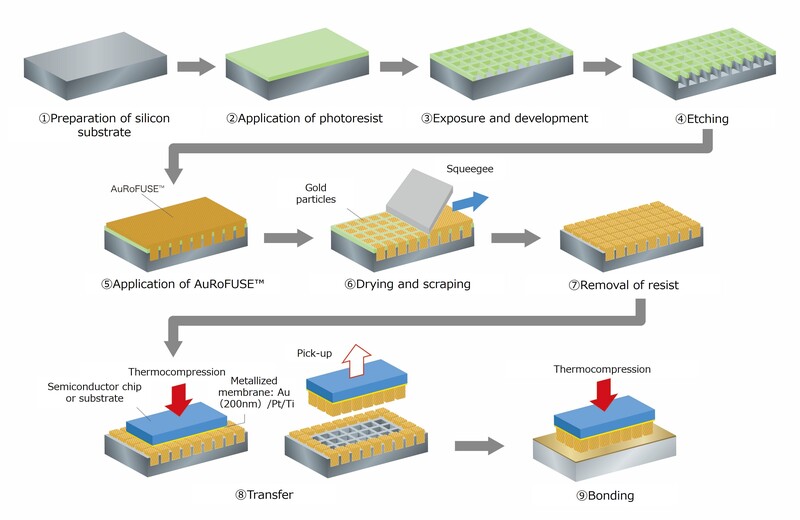
- ① Prepare a silicon substrate as a transfer substrate
- ② Apply photoresist on silicon substrate
- ③ Expose and develop to the desired pattern
- ④ Etch holes in the silicon substrate
- ⑤ Embed AuRoFUSE™ using a squeegee or similar tool
- ⑥ Dry AuRoFUSE™ at room temperature and under vacuum, and scrape off excess gold particles on the resist.
- ⑦ Removing the resist creates a transfer substrate
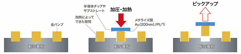
- ⑧ The object (semiconductor chip or substrate) on which gold bumps are to be formed is placed on the transfer substrate, and pressurized heating is performed at 10 MPa, 150°C, and for 1 minute. After that, the substrate is lifted vertically, and the gold bumps are transferred.
- ⑨ Bond the substrate after transfer at 20 MPa, 200°C, and 10 seconds of pressurized heating.
Example
<Results of Application to Ultra-Compact Double-Sided Cooling Power Module (Professor Yoshikazu Takahashi, Tohoku University)>
Using AuRoFUSE™ Preforms for the bonding of chip electrodes of modules incorporating power devices for inverters and substrate circuits has been found to contribute to improved thermal resistance compared to conventional solder. In addition, it has passed the Power Cycle Test, which is part of the evaluation standards for automotive power modules in Europe (AQG324).
| Test | Terms | Sintered Gold(Au) Bonding Technology: AuRoFUSE™ Preform | solder |
|---|---|---|---|
| Thermal Resistance | Cooling water: 10L/min | 0.98 for the entire system | 1.00 (Reference) for the entire system |
| Power Cycle | T jmax:175℃/T jmin:75℃ 2sec ON/18sec OFF |
60,000 cycles V on remains unchanged. |
60,000 cycles V increased by 3.2% compared to the initial version. |
This research was conducted by Tohoku University with the support of the Ministry of Education, Culture, Sports, Science and Technology under the “Research and Development Project for the Creation of Innovative Power Electronics” (Grant Number: JPJ009777). TANAKA PRECIOUS METAL TECHNOLOGIES has provided AuRoFUSE™ Preforms and served on the advisory board.
Related Companies
TANAKA PRECIOUS METAL TECHNOLOGIES and MEMS CORE leverage their respective strengths to provide materials and prototype and evaluate the implementation of preforms (Au bumps) in a mutually coordinated manner to establish a speedy development system.

MEMS CORE, INC. website: https://www.mems-core.com/index.html
Related Information

First, please make an Inquiry about the product.
For any questions regarding product specifications, pricing, delivery times, etc., please feel free to Inquiry here.