
Precious Metals Precursors for CVD/ALD Deposition
What are "CVD/ALD Precursors"?
These are film-forming materials used in CVD (chemical vapor deposition) and ALD (atomic layer deposition) processes, which were developed to accommodate the miniaturization and high performance of semiconductors. We develop a variety of CVD/ALD precursors, primarily ruthenium (Ru).
Development of high-purity precious metal precursors for next-generation semiconductors
Amid the semiconductor industry’s requirement for further miniaturization and improved durability, TANAKA seeks to reduce costs and achieve higher quality by improving the film deposition speed of ruthenium (Ru) precursors, and will contribute to the development of new advanced technologies enabled by semiconductors.
CVD = Chemical Vapor Deposition
ALD = Atomic Layer Deposition
Development and Provision of Precursors
We develop various CVD/ALD precursors, mainly Ru-based. For this purpose, we have CVD systems for producing semiconductor thin films and a variety of analytical instruments (FE-SEM, AFM, XRF, etc.) to evaluate them and provide purpose-specific precursor solutions.
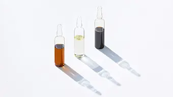
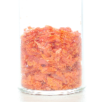
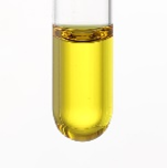
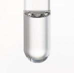
Examples of Precursor Products (Ru)
| Product Name | 外観 |
|---|---|
| DCR High-purity precursor for Ru film deposition |
|
| Rupta Oxygen-free Precursor for Ru Film Formation |
|
| TRuST High vapor pressure precursor for Ru film deposition |
|
As semiconductors have evolved, there are increasing expectations for Ru to promote further miniaturization of semiconductors because of its lower resistance and higher durability. With its superior characteristics, Ru is also being considered for use in transistor gate electrodes and DRAM capacitor electrodes.
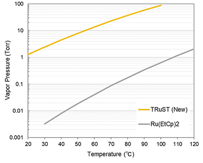
High vapor pressure precursor for Ru film formation: TRuST
Achieving the world's highest vapor pressures using liquid Ru precursors
A CVD/ALD precursor with a vapor pressure 100 times*higher than that of conventional liquid Ru precursors. This precursor will contribute to the improved performance and energy efficiency of the semiconductor devices used in smartphones, PCs, and the data centers where demand is expected to grow in the future.
*Experimental value obtained through TANAKA’s internal evaluation at room temperature
Features
- High vapor pressure even at around room temperature.
- Ru films with low resistance can be deposited as they easily decompose in reaction gases (hydrogen, oxygen, etc.).
- Has good adsorption efficiency on substrate surfaces due to its small molecules, enabling high film deposition speeds.
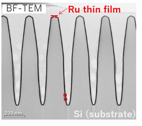
- Has excellent step coverage and can form films uniformly to their depths even on miniature structures with high aspect ratios.
Two-stage ALD process using TRuST
Prevents oxidation of substrates and achieves ultra-thin films of high quality and low resistance through a two-stage ALD process using oxygen and hydrogen
Two-stage film deposition process using TRuST
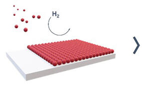

Step 1: Ru film formation using H2
Risk of surface oxidation of the substrate is reduced through hydrogen film formation
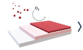
Step 2: Ru film deposition using O2
High-purity film deposition with a Ru purity of almost 100% through oxygen film deposition
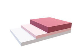
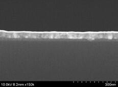
By first forming a base using hydrogen film formation, the Ru film formed by oxygen film formation on top of it is also smooth and dense, achieving lower resistance values than ever before.
- Using a two-stage film formation process, dense Ru films with low resistance can be deposited even in the ultra-thin film range.
- Since each process is carried out using the same raw materials and film formation temperatures, this contributes to reducing process costs and equipment investment costs.
Related Information

First, please make an Inquiry about the product.
For any questions regarding product specifications, pricing, delivery times, etc., please feel free to Inquiry here.