
Semiconductor Fabrication and TANAKA
Semiconductor Fabrication and TANAKA
TANAKA
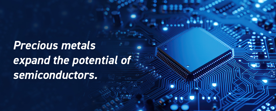
supports semiconductor innovation in the AI era with its precious metals technology.
The semiconductor market is rapidly growing due to the expansion of AI data centers and the evolution of physical AI (robotics, automation, and edge devices). Along with this, the importance of high-precision and highly reliable materials technology in the manufacturing processes of various semiconductor chips, including logic, memory, and power semiconductors, is increasing.
TANAKA provides materials and process solutions centered on precious metals from front-end to back-end (packaging and testing). Examples include CVD/ALD precursors and sputtering targets that support miniaturization, as well as Ag adhesives and bonding wires for packaging. Probe Pin materials contribute to precision testing.
In AI semiconductors and devices for high-performance computing (HPC), in addition to miniaturization and high integration, power efficiency and thermal measures are also challenges. Precious metal materials address these issues due to their excellent electrical conductivity, heat resistance, and reliability.
Furthermore, in order to promote sustainable semiconductor manufacturing, we are promoting the recycling of precious metals. We provide value as a partner to global semiconductor manufacturers, balancing reduced environmental impact with stable supply.
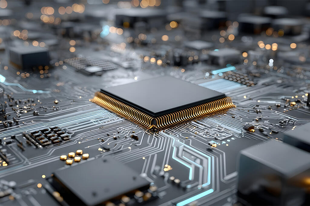
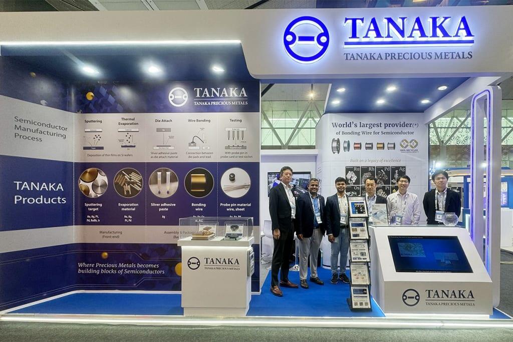
Semiconductor Manufacturing Process
As the performance of semiconductor devices evolves, the industry is facing increasing challenges related to heat management, bonding reliability, and testing accuracy. TANAKA addresses these challenges with a comprehensive lineup of materials designed for next-generation manufacturing.
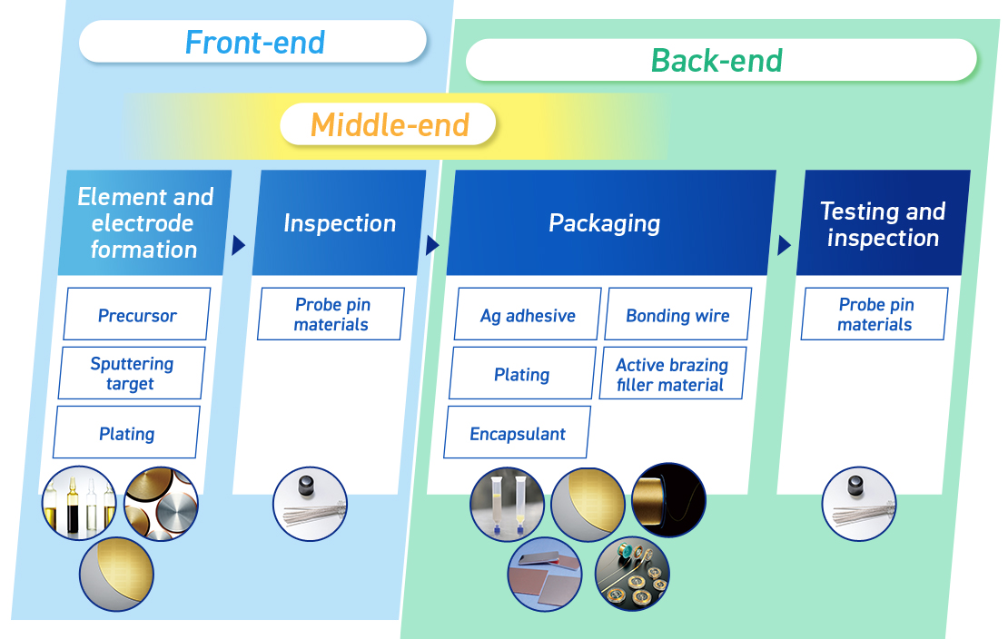
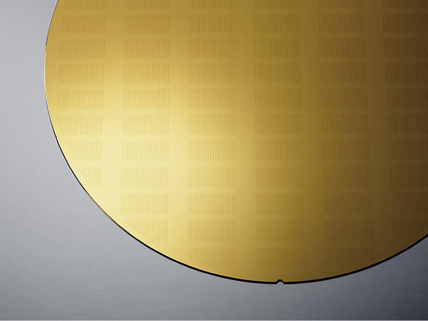
TANAKA's Products
-

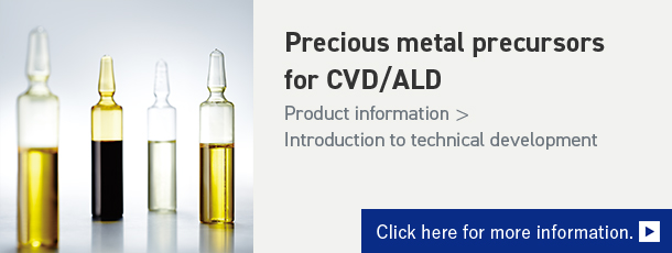
Precursor
We develop high-purity precious metal precursors, including ruthenium, for CVD/ALD processes. We offer precursors according to their intended use, with a lineup of thin film deposition equipment for semiconductors and analytical equipment for evaluation. We have also established recycling technologies for precursors during and after use, which can help reduce the cost of precious metal materials and alloys.
-
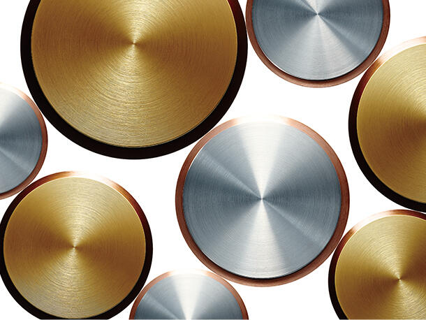
Sputtering Target
(Melting Method/Sintering)We use melting and sintering technologies to provide targets with various shapes, dimensions, and alloy compositions according to their intended use. We have a track record of products with high purity suitable for semiconductors. In addition, we recycle precious metals from used targets as well as from equipment and tools.
-
Plating Processes
We offer plating characteristics with high productivity and low cost according to their intended use. We pursue the matching of various wafer plating systems and chemical processes according to our customers' needs, from experimental and small-scale production to mass production systems, and provide them as total systems.
-
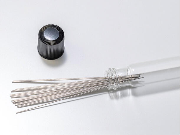
Materials for Probe Pins
We offer a variety of Probe Pin materials that simultaneously achieve low electrical resistivity, high bendability, and a wide range of hardness, taking advantage of the stable environmental resistance and electrical characteristics of platinum-based fine wires. This helps reduce deformation of Probe Pins due to wear during semiconductor testing, contributing to longer lifespans and lower costs of testing equipment.
-
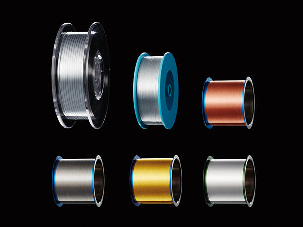
Bonding Wires
One of the world's leading suppliers of bonding wires. We offer a reliable range of products that always match the cutting edge of semiconductor technology, including gold, copper, silver, and aluminum wires.
-

Adhesive for die bonding
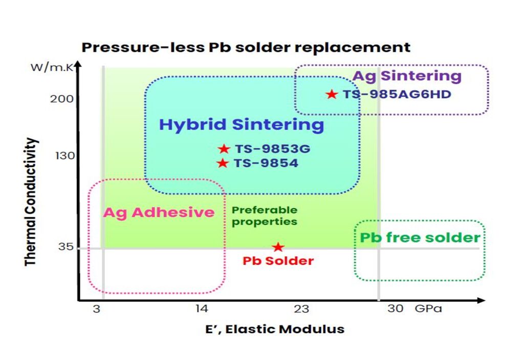
We offer a diverse lineup of products, with a focus on conductive adhesives. In particular, for power semiconductors, we provide products that meet the needs for high thermal conductivity (100 W/m·K or higher), high heat dissipation, and high reliability, depending on whether they are used with GaN, SiC chips, or as solder alternatives.
-
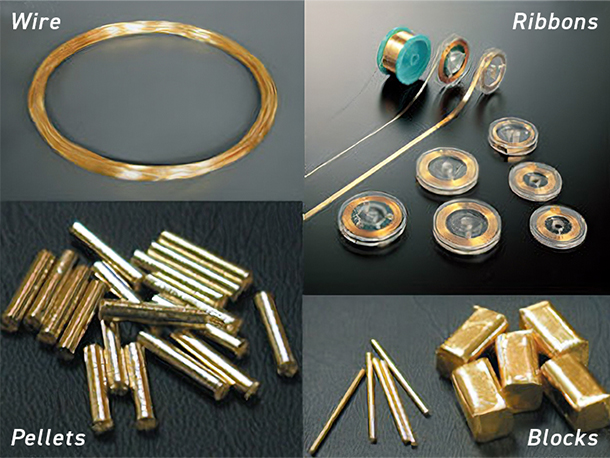
High-purity Materials for Evaporation, Joining and Sealing
We offer a wide range of products for use in bonding precision components and sealing gas. We can provide high-performance materials with reduced gas entrapment and oxidation of added elements in wire, ribbon, pellets, blocks, and spherical forms according to customer needs.
-
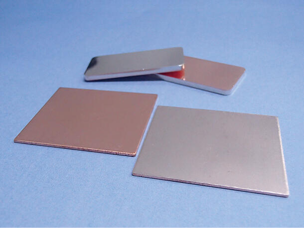
Active Brazing Filler Metals
Various types of ceramics, including oxide and nitride, can be brazed without metallization. Materials in which active brazing filler metal is combined with copper are also available, and these are expected to be used for ceramic circuit substrates for power devices and heat dissipation materials such as heat sinks.
-
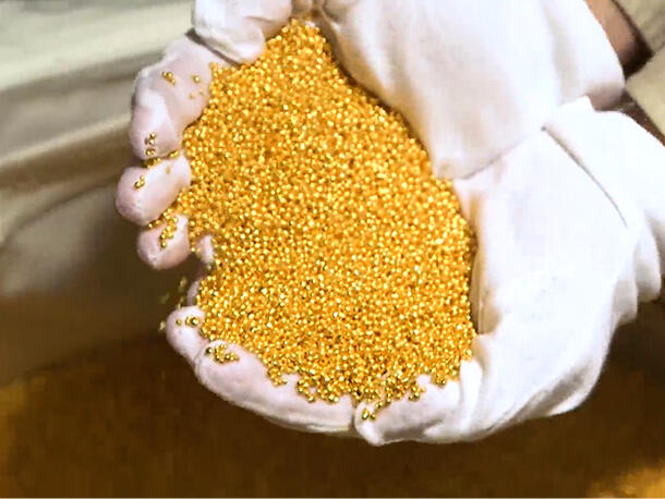
Precious Metal Recycling
Using advanced recycling and precious metal analysis technologies developed over many years, we recycle precious metals from production scraps in the manufacturing process and used industrial products. We contribute to reducing our customers' costs and promoting a Circular Economy.


Related Materials

Related Products


Semiconductors offer high capacity, high speed, and high reliability.
High performance, such as low power consumption, is required.
It continues to evolve every day.
The foundation of cutting-edge technology
Supporting semiconductors with materials
TANAKA
We will contribute through a variety of products.
Related Information
First, please make an Inquiry about the product.
For any questions regarding product specifications, pricing, delivery times, etc., please feel free to Inquiry here.