
TANAKA PRECIOUS METAL GROUP Supports Miniaturization of Chip Wiring and Promotes Recycling From General-Purpose to Cutting-Edge, Precious Metals Support the Future of Semiconductors (P2)
Ensuring a stable supply of rare materials
TANAKA PRECIOUS METAL GROUP has a long history in the semiconductor products business, having entered the business in the 1960s. It began by supplying gold wire for transistors, which has high conductivity, chemical Features, and is easy to process. Today, the group boasts one of the world's top shares in the supply of semiconductor bonding wire, including copper and aluminum products.
As semiconductor demand continues to grow, the minerals that precious metals are derived from have limited production regions and quantities. Only a group of precious metal professionals, such as the Group, can fulfill the role of providing the required precious metal materials in the necessary quantities and in a timely manner.
In addition, since precious metal materials are themselves rare in the supply chain of precious metal materials, systems for production and distribution with recycling in mind are extremely important. Precious metal recycling is one of the core businesses of the Group, which is promoting the global development of recycling sites. "The recycling of precious metal components from production scrap generated during the manufacturing process and from semiconductors that have reached the end of their life in the market has been a prerequisite for our company, which deals with rare materials," says Tsutomu Yamashita, who oversees the development of bonding wires at TANAKA ELECTRONICS. In response to recent social needs, TANAKA ELECTRONICS also offers gold bonding wires made from 100% recycled material. It can truly be said that the Group is a frontrunner in material recycling.
While the wire technology for general-purpose chips is in a period of maturity, the introduction of new technologies is essential for power semiconductors. Since large currents are used, aluminum wire, which is inexpensive and can form thick wiring, has often been used. However, with the practical application of SiC (silicon carbide)-based devices and improved heat resistance, thick copper wire has started to be used.
Reliable wire bonding is important for bonding wires. Depending on the material, hardness or softness may be required, and it is necessary to temper the material to make it easier to use while taking advantage of its characteristics. The Group has established a system for developing and supplying wires according to customer needs using its unique technologies and know-how.
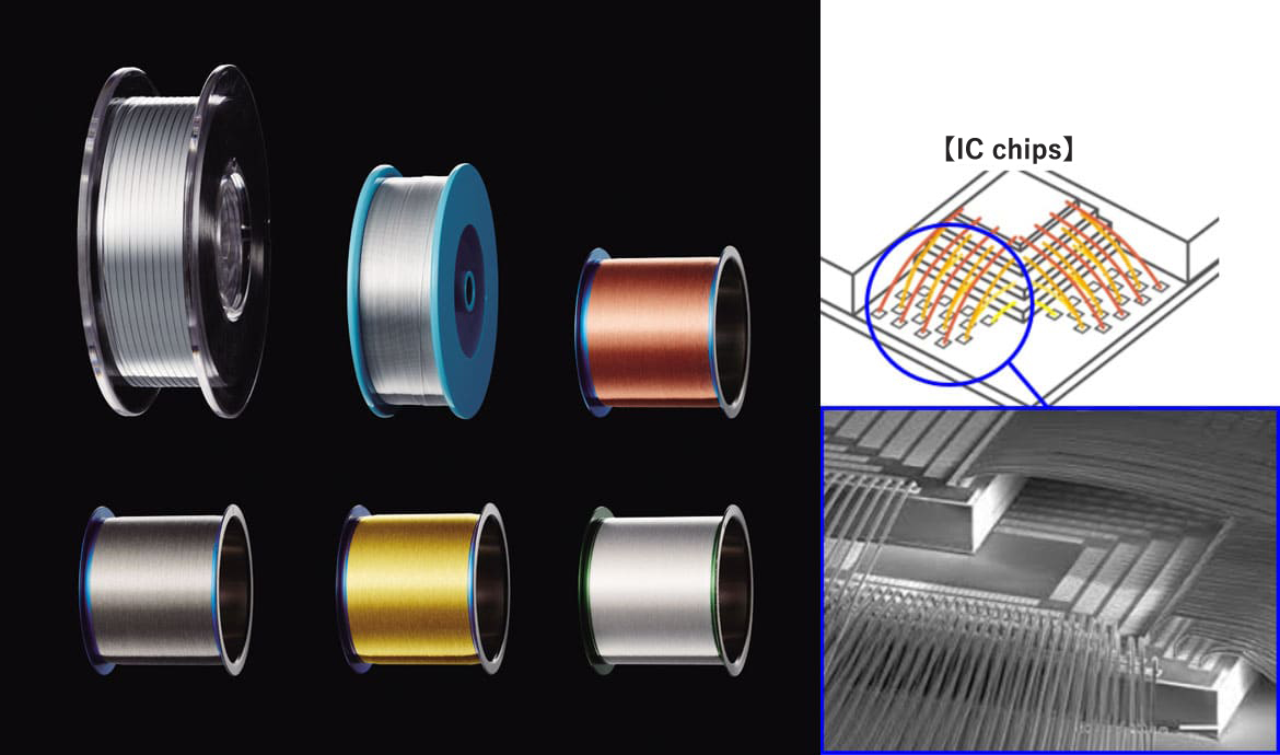
Bonding Wires
Mounting materials widely used in mass-produced general-purpose products,
Bonding Wire
Bonding wire is a conductive wire that connects the electrodes on semiconductor chips to packages and lead frames. Gold wire has mainly been used since the dawn of the semiconductor industry, but at present, except for some multilayer memory and automotive packages, copper wire with palladium coating is used. In recent years, among advanced chips, mounting technologies other than wire bonding, such as bumps, have started to be used; however, wire bonding is still widely used, especially for general-purpose products. The demand for wires continues to grow at a rate of several percent per year.
Supporting the Evolution of Semiconductors with the Power of Precious Metals
On the other hand, there are expectations for the use of new precious metals in the evolution of cutting-edge chips in the near future.
The width of the finest wiring formed on chips at the 1.4nm node will be less than 10nm, and in place of copper wiring, the introduction of ruthenium wiring is being considered. As wiring becomes finer, expectations for ruthenium are growing as it has lower electrical resistance and better properties than copper that are less likely to cause diffusion during high-temperature environments during operation.
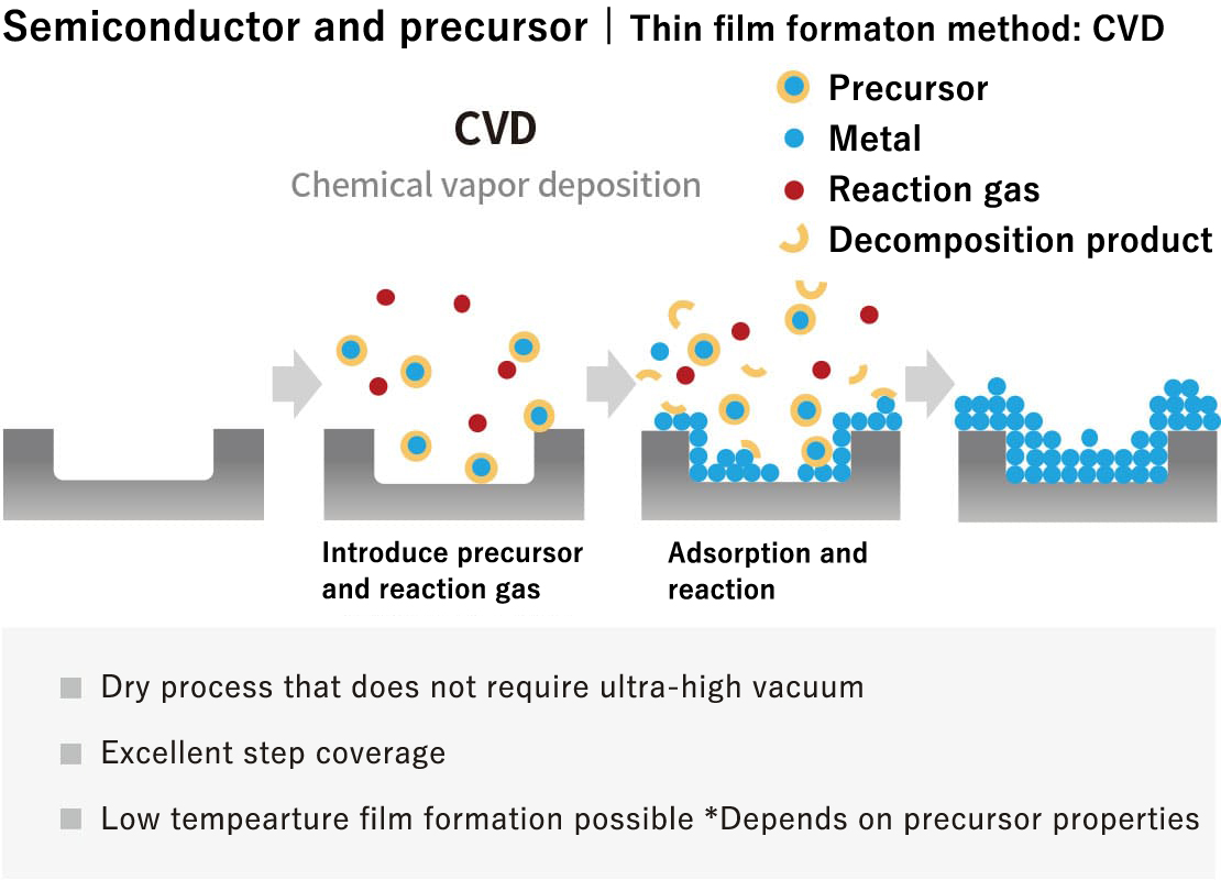
TANAKA PRECIOUS METAL GROUP develops and supplies precursors, which are materials for forming ruthenium thin films using CVD (Chemical Vapor Deposition) and ALD (Atomic Layer Deposition). One of its proprietary products, TRuST, has extremely high vapor pressure and can form high-quality ruthenium thin films with high uniformity and coating properties in the fine, deep grooves on chips. “The film formation methods and conditions vary for each semiconductor manufacturer, and the required specifications for precursors differ widely. Therefore, close collaboration with partner companies and equipment manufacturers is essential. We have been developing precursors and accumulating technology for over 20 years. With the recent evolution of semiconductors, I feel that the time has finally come for this technology to flourish in society,” says Hirofumi Nakagawa of TANAKA PRECIOUS METAL TECHNOLOGIES.
Ruthenium is a precious metal that is far rarer than gold and platinum. Moreover, the effective utilization rate of ruthenium during precursor production and film deposition processes is also low relative to the amount used. The Company has established technologies for recovery and reuse and is able to provide total solutions.
"In the semiconductor industry, which continues to change in both technology and business, we believe that it is of utmost importance to respond quickly and accurately to market movements. We will sense the demands of the times and accurately take in our customers' voices, making proposals that only a group of precious metals professionals can offer," says Naoko Abe of TANAKA HOLDINGS. The group's presence in the semiconductor industry is likely to grow even larger.
Precursor
Essential for miniaturizing chip wiring
Precursor for film formation
Precursor refers to a substance that serves as a preliminary stage for generating a target substance in processes such as film formation. In film formation processes using methods such as CVD and ALD, liquid precursors of organometallic compounds are gasified and introduced into the chamber, where they are simultaneously introduced with other substances and subjected to heat, plasma, oxygen gas, hydrogen gas, etc. to decompose them and undergo metal reactions to form thin films. Oxygen and hydrogen are used as reaction gases to promote the reactions. When forming thin films for wiring, it is necessary to use precursors with high vapor pressure after gasification that can form thin films uniformly in fine, deep grooves.
This article is a reprint of an article advertisement published in NIKKEI CROSS TECH (PR) starting November 25, 2024, with permission from Nikkei BP.
How was this article?
If you found this helpful, please share it.