CLOSE
About Elements
TANAKA is a leading company in the field of precious metals.
Advanced materials and solutions that support societal progress, the development stories behind them, the voices of engineers, and our management philosophy and vision—
Elements is an online media platform that shares insights that lead to a better society and a more prosperous future for the planet under the slogan “Mastering Precious Metals.”

A media platform by TANAKA
supporting societal progress with
advanced materials.


Search within Elements
Search by tags
India’s Semiconductor Ecosystem May Surpass China Over Time.”- Yutaka Ito, Natalie Abe, And Satoshi Teshima, TANAKA

Source: Electronics For You BUSINESS – News
Date: October 15 , 2025
Link: https://www.electronicsforyou.biz/eb-specials/indias-semiconductor-ecosystem-may-surpass-china-over-time-yutaka-ito-natalie-abe-and-satoshi-teshima-tanaka/
Think gold is just for jewelry? In semiconductors, it determines whether chips last or fail. At SEMICON India ’25, TANAKA`s leaders Yutaka Ito, Natalie Abe, and Satoshi Teshima share with EFY’s Akanksha Sondhi Gaur and Nidhi Agarwal how ultra-pure bonding wires and recycled metals are making materials smarter, supply chains stronger, and positioning India as a true architect in the global semiconductor mission.
Q. Can you outline your core offerings and expertise?
A. We provide a broad range of precious metal products, focusing mainly on electronics and semiconductors. Precious metals such as platinum, gold, silver, palladium, iridium, and ruthenium, each chosen for their outstanding conductivity, reliability, and stability. These metals aren’t just shiny, they’re critical for everything from chip packaging to automotive electronics.
For the semiconductor market, we began by specializing in ultra-high-purity materials, such as gold wire with up to 99.99% purity, offering both superior electrical performance and long-term durability. Over the years, we didn’t stop at gold. We expanded into copper, palladium-coated copper, silver and aluminum wires, evolving into a global leader in bonding wire for semiconductor packaging.
Q. Why is the demand for these materials rising in advanced electronics?
A. Advanced packaging technologies such as fine-pitch wire bonding and high-frequency chip integration require clean surfaces and predictably conductive wires. Ultra-pure gold wires make this possible by allowing electrons to flow with minimal resistance.
For power electronics applications, thicker aluminum and copper wires or ribbon are employed. Their larger cross-section provides better current-carrying capacity and improved thermal robustness, which is essential for wide-bandgap devices such as silicon carbide (SiC) and gallium nitride (GaN).
Meanwhile, in advanced integration methods like in chiplet and 3D-packaging, high-density interconnects rely on microbumps and hybrid bonding, supported by our advanced plating solutions that ensure fine-pitch reliability and compatibility with diverse substrates. Complementing these interconnect technologies, our silver adhesive pastes provide robust die attach and efficient heat dissipation, maintaining reliability under thermal stress to meet the performance and reliability demands of next-generation devices.
This article was published on EFY BUSINESS. Further information can be found here:
Learn more… (Electronics For You BUSINESS)
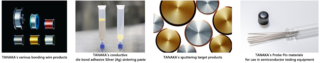
Image reference: TANAKA to Showcase Advanced Semiconductor Materials in its Inaugural Participation at SEMICON India 2025 | TANAKA
Related Information
