Case Study
Improving Material Usage Rate Through Recycling
Compact and lightweight – the next generation technology development proposition.
Helping projects succeed through innovative material recycling ideas.
Chipmaker;Y Inc.
 Miniaturization of the wiring does not go well and impossible to commercialize
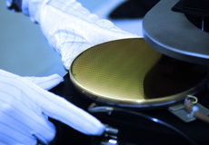
Manufacturers face the critical issue of making electronic equipment smaller and lighter. Semiconductors must then also be made smaller and with greater capacity in order to accommodate this electronic equipment, leading to many challenges, such as the miniaturization of wiring.
Y Inc. was also occupied with developing next-generation devices to answer the demands from manufacturers.
Mr. K, representative from the R&D Division explained: “As compactness is taken for granted nowadays, our company has had to develop devices with greater data capacity. However, we were faced with the technological challenge of miniaturizing the wiring. Miniaturization caused flaws such as yield deterioration to occur during the process of wiring formation and we were unable to manufacture devices according to our designs, making productization impossible.”
In addition, the lengthy research and development put pressure on costs and as delivery dates drew near there was no time to restart development from scratch – Y Inc. was in trouble.
 Utilize each material’s properties for successful development!
Mr. K, who asked a colleague from another department if they had made any breakthroughs, was introduced to a TANAKA representative. When Mr. K explained the product under development, the representative suggested using a purer version of the same material. He further explained that TANAKA had the capability to supply materials with a high degree of purity and all impurities removed.
Mr. K therefore decided to manufacture a sample made from material of a higher purity than that previously used. As a result, the higher purity material eliminated the problematic flaws and the subsequent product was finally improved enough to release as a commercial product.
Successful development marred by unforeseen costs…
However, Y Inc. encountered an unforeseen pitfall when considering full-scale productization: greater-than-anticipated costs caused by a large volume of material loss in the device manufacturing process. “Under normal conditions, we were only actually using 10% of the materials. The remaining materials were all going to waste so it would have been too costly to implement mass production in this state,” said Mr. K.
Mr. K discussed the cost issue with TANAKA representative and he received a surprising response.
Cut costs and losses by recycling materials
The answer he received: “Our process doesn’t waste materials so you don’t need to worry about costs.” With TANAKA recycling system, 90% of materials that had been thrown away until now were re-refined to the same purity as that of the original new materials and were able to be re-used. Y Inc. was given a total cost proposal taking into account the material utilization rate with recycling and the company succeeded in cutting the cost of the wiring formation process by 30%. This brightened prospects for stable supply after productization and the manufacturer that had requested the product was also extremely satisfied with the goods they received.
Mr. K said, “Being in the development division, I thought that I knew everything. But of course it turned out that it was best to go to a specialist for the best results. I realized that when it comes to materials, one should consult a materials specialist.” Mr. K also said that he would keep consulting TANAKA for advice from the point of materials selection when developing devices in the future.