
The evolution of power semiconductors that support the promotion of GX and the spread of EVs. This article examines the current state of material development that underpins this evolution.
- The two major roles of power semiconductors are power supply control and motor control.
- Power semiconductors to curb power consumption from the spread of generative AI
- Next-Generation Power Semiconductors Using SiC and GaN
- What are the intentions of the U.S., China, and India?
- TANAKA PRECIOUS METAL GROUP—Maximizing the Potential of Precious Metal Materials
TANAKA PRECIOUS METAL GROUP—Maximizing the Potential of Precious Metal Materials
Minamikawa: What role do you think the TANAKA PRECIOUS METAL GROUP should play under these circumstances?
Abe: We are a manufacturer of advanced materials using precious metals. One of our roles is to maximize the potential of precious metal materials. Another is to contribute to the industry using process technologies developed through many years of technological development.
The first point is that we develop advanced materials that utilize the unique qualities of precious metals, such as low resistance, high electrical conductivity, minimal chemical change, and reliability.
We have limitless technological development for imparting functionality, not only using pure materials but also using alloys and adding additives. Although precious metals are perceived as expensive, we respond to industry needs while drawing a roadmap for reducing costs, such as reducing the precious metal content.
Another area is materials other than precious metals that we have handled over our long history, with bonding wires for power semiconductors being a prime example. We offer products made from aluminum and copper. Originally, we provided gold wire for semiconductors, but we applied our process technology to develop and mass-produce aluminum bonding wire faster than any other company.
TANAKA PRECIOUS METAL GROUP's strength is its ability to apply its technological development capabilities centered on precious metals to offer materials suited to specific applications even when using materials other than precious metals.
We will continue to develop next-generation advanced materials ahead of the times while keeping track of trends across the industry, including those of end applications.
Namikawa: While this is not limited to semiconductors, we are entering an era where we are using AI to develop new materials.
I hope that you will take on such challenges, as they may lead to the creation of new materials beyond the realm of semiconductors.
ABE: Thank you for the great idea.
TANAKA PRECIOUS METAL GROUP will celebrate its 140th anniversary in July 2025. In aiming to become a 200-year company, a new exploration team called “Dock2085” has been established within the Group.
At this stage, we are conducting research on the emergence of interesting functions, even though the application is not yet known, and exploring business fields where precious metals have not been involved. We will promote both the strengthening of our current business and seed-sowing activities for the future.
Finally, thank you for your comments, which feel like support for us. We will continue to strive to be one of the companies that can contribute to the semiconductor industry.
TANAKA's Products for Power Devices Offering Total Solutions
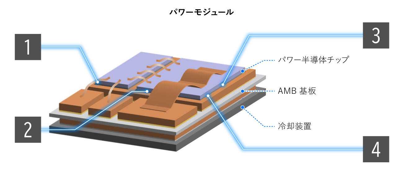

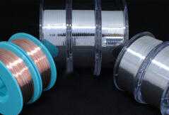
Bonding Wires
Al Wire/Ribbon
- High bondability
- High humidity resistance
Cu Wire/Ribbon
- Excellent electrical conductivity
- Excellent cutting current


Die Bonding Material
Ag Adhesive
- Good adhesion to bare Si
Hybrid Ag Adhesive
- High thermal conductivity
- High reliability
Sintered Pure Silver
- High thermal conductivity
- High thermal bonding strength

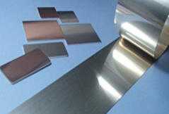
Active Brazing Filler Metal/Copper Composite Material
Thick Cu Circuit Formation
- Etching-free method
- Can be used for thin foil of solder material
Binderless
- Easy maintenance of the furnace
Reduced heat treatment time
- Low melting solder
 【Various Electrodes and Metallized Layers】

Plating Processes
Metallized layer for bonding pads
- Ni/Pd/Au, Ni/Au, Ag, etc.
- Appropriate suggestions for the combination of bonding wire and pad materials
- Achieving high reliability and high production efficiency
Rear-side electrodes for ohmic contacts
- Ni/Au and others
- Suppresses wafer warpage under low stress
- Good bondability for die attachment
Lead frames, copper clips, and for PCBs
- Ni/Pd/Au, etc.
- Prevention of Ni layer diffusion
- Thinning Au layer to reduce overall costs

Sputtering Target
Various precious metal targets and alloy targets
- Pure precious metal targets such as Au, Ag, Pt, Pd, and Ir
- Precious Metal Alloy Target
- High-purity targets suitable for various electrodes and metallization layers
- Film formation without defects such as pinholes, oxides, and gas
- Silver alloy targets with high environmental resistance (sulfuration and humidity resistance)

Related Information
Technology Trend and Advanced Packaging Material for Power Device
As energy-saving technologies for smartphones and electronic devices, next-generation mobility such as EVs, base stations, and power control for renewable energy continue to advance, the technological development of power semiconductors will increasingly require higher output and efficiency.
We will introduce cutting-edge materials and packaging technology trends to address issues such as high heat dissipation, high heat resistance, bonding reliability, and miniaturization.


How was this article?
If you found this helpful, please share it.