
The Strategic Role of Precious Metals in Defining Semiconductor Performance
Source: EE Times Asia
Date: May 1, 2026
Author: Yasutaka Ihara, Director & Corporate Officer, TANAKA PRECIOUS METAL TECHNOLOGIES Co., Ltd
Link: The Strategic Role of Precious Metals in Defining Semiconductor Performance - EE Times Asia
Semiconductor performance is shifting from transistor scaling to materials innovation amid rapidly rising AI-driven complexity demands. The semiconductor industry’s long-standing reliance on transistor scaling is giving way to a more complex reality—one where system-level performance is increasingly constrained, and enabled, by materials.
According to the Semiconductor Industry Association (SIA), global semiconductor sales reached $627 billion in 2024 and are projected to exceed $1 trillion by the end of the decade, driven largely by artificial intelligence (AI), high-performance computing (HPC), automotive electrification, and industrial digitalization. Meanwhile, International Data Corp. (IDC) estimates that AI-related semiconductor demand alone will grow at a double-digit CAGR through 2030, reflecting the rapid expansion of hyperscale data centers and edge AI systems. For its part, Omdia, a global technology research and advisory firm specializing in semiconductor and electronics market analysis has significantly raised its initial semiconductor revenue growth forecast to 62.7% for 2026. This growth is also being reinforced by regional expansion in semiconductor manufacturing, particularly in Southeast Asia, where increasing demand for AI-related applications is contributing to sustained momentum in materials usage.
This growth is not just increasing volume—it is reshaping design priorities. Power density is rising sharply, thermal budgets are tightening, and reliability expectations are extending over longer operational lifetimes, particularly in automotive and industrial environments. In this context, materials—especially precious metals such as gold, silver, palladium, platinum, iridium, and ruthenium—are no longer passive enablers. They are now central to determining how much of a device’s theoretical performance can be realized in practice.
Why precious metals
Because of their intrinsic physical and chemical properties, precious metals occupy a unique position in semiconductor manufacturing.
Gold, for instance, remains unmatched in corrosion resistance, bond reliability, and malleability, making it indispensable in fine-pitch interconnects and high-reliability packaging. Meanwhile, silver offers the highest electrical and thermal conductivity among metals, making it critical for die-attach and heat dissipation applications.
While palladium provides a balance of hardness, conductivity, and oxidation resistance, ruthenium and platinum-group metals are increasingly important in front-end processes, where thin films must combine low resistivity with high durability in aggressively scaled structures.
At the same time, the increasing reliance on these materials is bringing greater attention to how they are procured, used, and recovered. As semiconductor manufacturing scales, the ability to manage precious metals efficiently—both in terms of consumption and lifecycle—has become an important consideration alongside performance.
Material performance required in the AI era
“As compute density rises, heat generation becomes more concentrated, power delivery becomes more demanding, and long-term reliability at the package and interconnect level becomes more critical,” says Yasutaka Ihara, Director & Corporate Officer at TANAKA PRECIOUS METAL TECHNOLOGIES Co., Ltd,
adding that the industry’s shift toward AI and HPC has intensified the importance of these properties.
“AI workloads and hyperscale data center expansion are changing semiconductor design priorities in a very fundamental way,” says Ihara. “For many years, the industry was primarily driven by transistor scaling, but in AI and HPC, the challenge is increasingly about how to extract system-level performance from highly integrated devices operating under severe thermal and electrical conditions. As compute density rises, heat generation becomes more concentrated, power delivery becomes more demanding, and long-term reliability at the package and interconnect level becomes more critical.”
Ihara adds that materials now have a much more direct effect on achievable performance of semiconductors. “It is no longer enough for a material to simply function as a passive interconnect or joining medium. Die-attach materials, bonding materials, thin films, plating layers, and testing materials all influence how effectively heat can be removed, how stably current can be handled, and how reliably the device can operate over time,” he says. “In AI and HPC systems, where high utilization can continue for long periods, and the ability to maintain electrical and mechanical stability under sustained thermal stress is extremely important.”
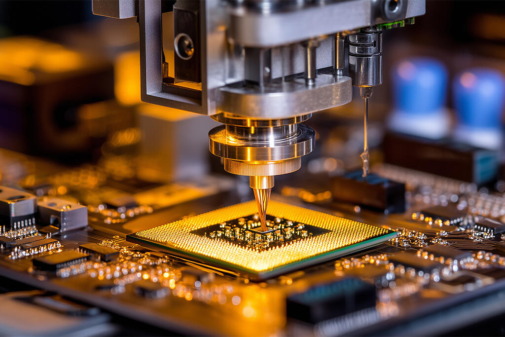
TANAKA's Materials Technology Supporting the Entire Semiconductor Manufacturing Process
As device architectures become more demanding, the materials challenge has become more central. From TANAKA’s perspective, this is exactly where advanced materials become more valuable. Precious metal-based materials are being used not only because of their conductivity, but because they can contribute to a broader balance of electrical performance, heat resistance, corrosion resistance, and reliability.
TANAKA has positioned its semiconductor materials business across the full manufacturing flow to help manufacturers address these industry challenges. With more than 140 years of experience in precious metals, the company has built capabilities spanning procurement, refining, purity control, materials design, and application development. Its semiconductor portfolio now covers front-end processes, packaging, and testing.
For instance, TANAKA provides high-purity precious metal precursors for CVD and ALD deposition processes, including ruthenium-based materials, as well as sputtering targets designed for low-resistance and high-durability films, in thin-film formation.
In packaging, its materials portfolio addresses both interconnect and thermal challenges. Bonding wire solutions span gold and gold-alloys, silver, copper, and palladium-coated copper. TANAKA also provides thicker aluminum and copper wires and ribbons for power devices. Precious metal plating technologies are engineered to provide corrosion resistance, stable contact resistance, and durability under high current density and thermal cycling conditions in advanced semiconductor packages.
Supporting sustainability
As semiconductor manufacturing becomes more resource-intensive, the role of precious metal recycling is shifting from sustainability initiative to operational necessity. In addition, continued volatility in precious metal prices is reinforcing the importance of recycling and material efficiency, as manufacturers seek to mitigate cost exposure while maintaining stable supply.
TANAKA has integrated these capabilities into a closed-loop system that spans recovery, refining, and remanufacturing.
“Recycling in this context is not only about sustainability,” Ihara says. “It is about quality control, supply stability, and efficient resource utilization. In that sense, closed-loop material flow is already becoming part of mainstream industrial practice.”
These solutions support applications in next-generation semiconductors and power electronics while contributing to initiatives toward a circular use of precious metals.
This article was reprinted from an article published in “EETIMES ASIA” on May 01, 2026, with permission from EETIMES ASIA. This article was translated by TANAKA from EETIMES ASIA with their permission.
This article was published on EETIMES ASIA. Further information can be found here:
Read more (EE Times Asia)
Related Information

Semiconductor Fabrication and TANAKA
Since its establishment in 1885,TANAKA has advanced hand-in-hand with Japan’s manufacturing industry as a specialist in precious metals.
How was this article?
If you found this helpful, please share it.