Precious Metal Film Formation Methods
Plating Processes

We can suggest high-performanceplating processes.
We offer various plating processes, including those using precious metal plating solutions, for various applications from semiconductor components to decorative articles. We offer highly productive plating processes with plating characteristics appropriate for their intended use.
Gold electroplating
PRECIOUSFAB Au series
The superior bondability, heat resistance, and solderability of this series make them ideal for semiconductor components. Excellent thickness uniformity at a low gold concentration, enabling reduced Au consumption.
PRECIOUSFAB Au-GB series
Gold electroplating process for wafer bumps. This series has excellent thickness uniformity, enabling plating with a high current density and low operation temperatures.
MICROFAB Au series
Non-cyanide Au plating for wafers. This series provides excellent properties for bump and fine pattern formation.

| Process name | Application | Features |
|---|---|---|
| PRECIOUSFAB Au 8400 | Bonding pad areas | Good uniform electrodeposition, Neutral cyanide |
| PRECIOUSFAB Au-MLA300 | Low gold concentration, Ni elution prevention, Neutral cyanide |
|
| PRECIOUSFAB Au-GB5 | Wafers (bump) | Low operation temperature, Neutral cyanide |
| MICROFAB Au310 | Wafers (wiring) | Very fine surface roughness, Neutral non-cyanide |
| MICROFAB AuFL2100 | Low gold concentration, Neutral non-cyanide |
|
| MICROFAB Au660 | Wafers (bump) | Low hardness, high-speed, Neutral non-cyanide |
| MICROFAB Au3151 | High hardness, high-speed, Neutral non-cyanide |
Gold alloy electroplating
PRECIOUSFAB HG series
Excellent electrical properties, abrasion resistance, corrosion resistance, and solderability. This series is suitable for connectors and other electronic components.
PRECIOUSFAB GT series
Electrolytic gold-tin alloy process. This series allows easy adjustment of alloy ratios, making it possible to adjust them according to their melting temperatures.
PRECIOUSFAB GS series
Electrolytic gold-silver alloy process. This series has both the corrosion resistance of gold and reflectivity of silver, making them ideal for LED components.

| Process name | Application | ||
|---|---|---|---|
| Au-Co | PRECIOUSFAB HG-GVC | Connectors, PWB | Acidity cyanide |
| PRECIOUSFAB HG-ICC7 | Ni barrier property, Acidity cyanide |
||
| FINE BARRIER 7000 | Ni barrier property, Acidity cyanide |
||
| Au-Ni | PRECIOUSFAB HG-GVN | Connectors, PWB | Acidity cyanide |
| PRECIOUSFAB HG-ICN100 | Ni barrier property, Acidity cyanide |
||
| Au-Sn20% | PRECIOUSFAB GT1000 | Alternative to coalescent | Acidity cyanide |
| Au-Ag50% | PRECIOUSFAB GS3000 | Lead frames | Alkali cyanide |
Gold strike plating
PRECIOUSFAB Au-ST
With “Au-ST400 (Chlorine free),” stainless steel and such in particular can be plated directly in a strongly acid strike bath.
MICROFAB Au NX-ST
Non-cyanide type strike bath.
| Process name | Application | Features |
|---|---|---|
| PRECIOUSFAB Au-ST100 | General use | Acidity cyanide |
| K-130AF | Acidity cyanide, Mildew-proofing | |
| PRECIOUSFAB Au-ST400 | SUS materials | Chlorine-free, Strong acidity cyanide |
| N-205 | High gloss, Strong acidity cyanide | |
| MICROFAB Au NX-ST | Wafer | Neutral non-cyanide |
Electroless gold plating
IM MEISTER Au series
Excellent adhesion and solder wettability on electroless Ni plating.
“IG100” develops uniform film thickness on Pd film.
CERAGOLD series
Self-reduction type thick Pb-free electroless gold plating process.
SUPERMEX series
Non-cyanide electroless gold plating process applied to electrolytic and electroless Ni plating.

| Process name | Application | Features |
|---|---|---|
| IM MEISTER Au1100S | Bonding pad areas | Immersion thin plating, Cyanide |
| IM MEISTER AuFX5 | Immersion thick plating, Cyanide | |
| IM MEISTER Au-IG100 | Uniform immersion thick Pd plating, Cyanide |
|
| IM FAB Au-IGS2020 | Uniform thick Ni plating, immersion, non-cyanide |
|
| ATOMEX | Ceramic parts, etc. | Immersion thin plating, Cyanide |
| CERAGOLD 6070 | Reduction thick plating, Pb-free, Cyanide |
|
| SUPERMEX 250 | Wafers, general use |
Immersion thin plating, Non-cyanide |
| SUPERMEX 850 | Reduction thick plating, Non-cyanide |
Silver plating
■Cyanide type
| Process name | Application | Features |
|---|---|---|
| Ag-10 | General use | Hard, High cyanide |
| LED BRIGHT Ag-20 | LEDs and others | Gloss, High cyanide |
| SP-4000 | Lead frames | Under high current density, Low cyanide |
■Non-Cyanide type
| Process name | Application | Features |
|---|---|---|
| PRECIOUSFAB Ag4730 | Wafer | Non-cyanide |
Platinum group plating
PRECIOUSFAB Pd series
The “AD series” is a palladium plating process with less ammonia odor, which is friendly to the work environment and offers excellent corrosion resistance at high temperatures.
PRECIOUSFAB Pt series
Platinum plating process that enables thick plating with low stress and crackless.
PRECIOUSFAB Rh, Ru, Ir
Plating process that enables decorative plating for industrial use.
| Process name | Application | Features | |
|---|---|---|---|
| Pd | Lead frames (Pd-PPF) |
Thin-film high heat resistance | |
| PRECIOUSFAB Pd-ADG860 | |||
| PRECIOUSFAB Pd82GVE | Connectors | Pd-Ni 20% alloy | |
| PRECIOUSFAB PC200 | Pd-Co 20% alloy | ||
| MICROFAB Pd700 | Wafers (bump) | Neutral, thick plating | |
| Pt | PRECIOUSFAB Pt2000 | Electronic components etc |
Acidity, High corrosion resistance |
| PRECIOUSFAB Pt-SF | Alkaline, Thick platingy | ||
| Rh | PRECIOUSFAB Rh200 | Low stress, High hardness | |
| PRECIOUSFAB Rh2000 | High corrosion resistance High hardness |
||
| Ru | PRECIOUSFAB Ru1000 | Acidity, Low Ru concentration | |
| Ir | PRECIOUSFAB Ir300 | High hardness | |
Examples of applications (Power device modules)
■Plating for bonding pad
-
Part Metal ① Bonding Wire Al, Au, Cu, PCC, Ag ② Plating on Bonding Pad Ni/(Pd)/Au or Ag Bonding Pad Al, Cu 
We offer optimal plating conditions with excellent bondability for various combinations of bonding wires and bonding pads.
Ni/Au plating (Ni thickness 5um / Au thickness 0.05um)
Φ50um pad

Ni/Pd/Au plating (Ni thickness 5um / Pd thickness 0.1um / Au thickness 0.05um)
□100um pad


- Limit corrosion and diffusion of Ni plating through the use of Pd plating
- Offer a comprehensive set of optimal processes, from the pretreatment conditions to the Au plating process
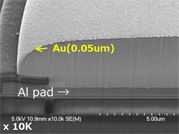
■Rear-side electrodes for ohmic contacts
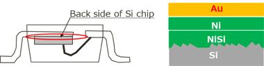
MICROFAB ELN520 – Plating process for ohmic contact on back of Si in vertical devices
- For Si backside ohmic contact of vertical devices including diodes
- Nickel silicide alloy layer is formed by sintering after directly electroless Ni plating to back side of Si.
Process for formation on back side of Si
| Process | Product Name | |
|---|---|---|
| 1 | Pretreatment | – |
| 2 | Catalytic activation | – |
| 3 | Electroless Nickel plating | MICROFAB ELN520 |
| 4 | Drying, Sintering | – |
| 5 | Electroless Gold plating | IM FAB Au-IGS4200 |
- Ni deposit has low stress, possible to suppress wafer warpage after plating.
- By electroless Au plating on Ni, the die attach bondability is good.
■Metalized layers such as lead frames, copper clips, and PCBs

TANAKA’s Pd plated coating has excellent barrier performance and can be expected to improve heat resistance property as a thin film.
Plating Processes for Pd-PPF
*…Palladium Pre-Plated Frame
| Electrolytic Ni | GALVANOMEISTER Ni100 |
| Electrolytic Pd | PRECIOUSFAB Pd series |
| Electrolytic Au | POSTFLASH 100 |